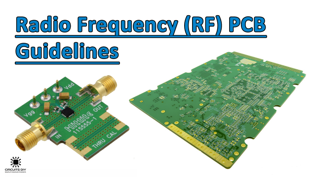
Introduction
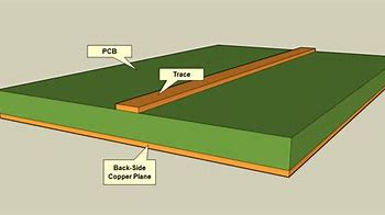
Signal traces are often referred to as the copper wiring that enables the connectivity between the components on the boards. In other words, it allows the current to flow through the circuit. It is the copper foil that does not get removed after the etching process. Usually, the copper foil is used as a signal trace but, aluminum and gold can also be used for this matter. These traces are very thin and are separated from each other by less than the half-meter space on the board. To understand signal traces on a printed circuit board, one must have to understand different tracing parameters.
Trace Width
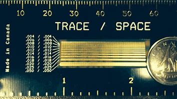
Trace widths are simpler yet difficult parameters of Printed circuit boards. It defines the current carrying capacity of the PCB. In past, larger trace widths were used according to their needs. But, with the evolvement of time and the evolution of PCB, it gets changed. Now, the width is calculated through width calculators while designing PCB. Both signal and power boards require the calculation. Most fabricators use a trace width of 6 mils, however, for high technology boards, they can go for 2.5 miles or less.
Trace Length
Trace length is also one of the parameters of signal traces. The PCB trace length process ensures that two or more traces are of the same length. The matching of two traces is necessary for the arrival of the pulse timings. Mostly, designing software provides the PCB traces of 1oz per 0.35mm. Remember, the length of these traces should not be comparable with one-tenth of the shortest frequency of the signal. Also, know that short but wider traces are more promising and preferable.
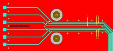
Trace Spacing
Some rules must have to be followed for trace spacing. Know that the traces between the pads under small surface components may have minimum to metal spacing but may also cause problems. traces that are close to each other can get shorted and damage the board and the device too. Therefore, traces and vias should not be too close to each other. copper weight is also counted while tracing. the higher weight needed minimum spacing. However, the higher weight is not preferable, hence not recommended.
Trace Resistance
We know that every material has some resistance, therefore PCB trace material has also some resistance which needs to be calculated. If the resistance is not calculated, it may create some design issues. Measuring the trace resistance is not difficult as it only requires the formula that is derived from the om=hms law. The formula is:
R = (ρ * L / (T * W)) * (1 + α * (TAMB – 25 °C))
Conclusion
Signal traces are like the wires that connect the components on the Printed circuit board. However, there are some parameters of signal traces that ensure the trace quality and its impact on the board and circuit. Thus, It’s not very difficult to calculate these parameters. Also, sometimes the trace can get damaged, disconnected the components, and lost continuity. For this purpose, a multimeter is used to check the continuity and work accordingly.