Contents
hide
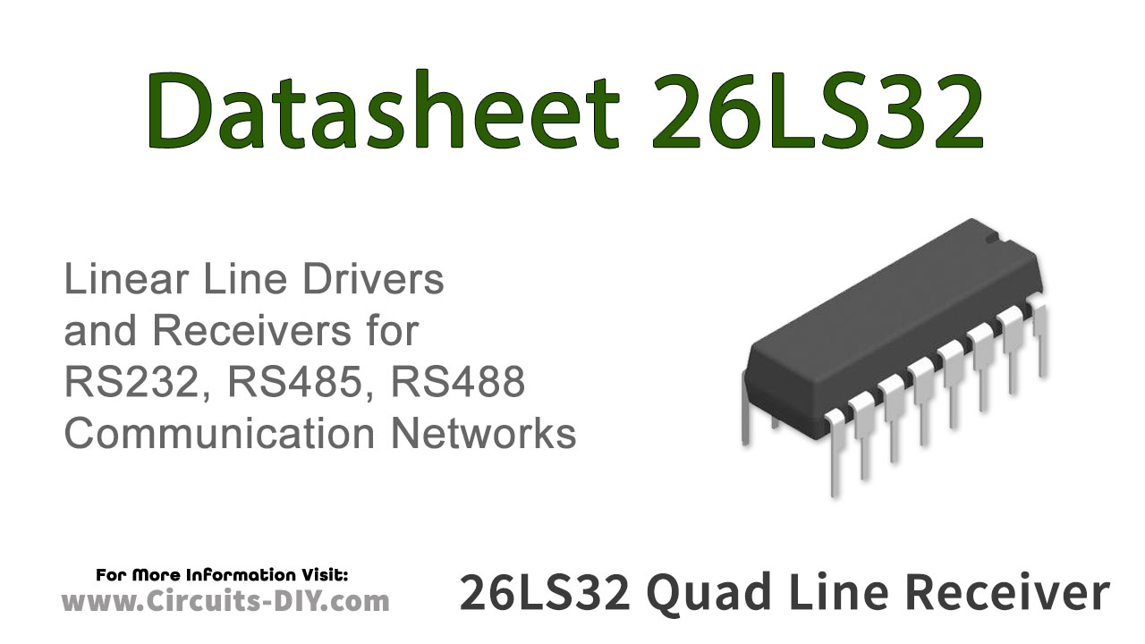
26LS32 Receiver features four independent receiver chains which comply with EIA Standards for the Electrical Characteristics of Balanced/Unbalanced Voltage Digital Interface Circuits. Receiver outputs are, three–state structures which are forced to a high impedance state when Pin 4 is a Logic “0” and Pin 12 is a Logic “1.” A PNP device buffers each output control pin to assure minimum loading for either Logic “1” or logic “0” inputs.
In addition, each receiver chain has internal hysteresis circuitry to improve noise margin and discourage output instability for slowly changing input waveform
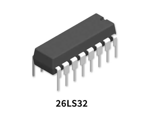
26LS32 Pinout
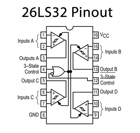
26LS32 Pin Configuration
| Pin No | Pin Name | Description |
|---|---|---|
| 1 | IN A1 | Input Pin A1 |
| 2 | IN A2 | Input Pin A2 |
| 3 | OUTA | Output Pin A |
| 4 | 3 STATE CONTROL | 3 State Pin Control PIN |
| 5 | OUT C | Output Pin C |
| 6 | IN C1 | Input Pin C1 |
| 7 | IN C2 | Input Pin C2 |
| 8 | GND | Ground Pin |
| 9 | IN D1 | Input Pin D1 |
| 10 | IN D2 | Input Pin D2 |
| 11 | OUT D | Output Pin D |
| 12 | 3 STATE CONTROL | 3 State Pin Control PIN |
| 13 | OUT B | Output Pin B |
| 14 | IN B1 | Input Pin B1 |
| 15 | IN B2 | Input Pin B2 |
| 16 | VCC | Collector Supply Voltage |
26LS32 Key Features
- Four Independent Receiver Chains
- Three–State Outputs
- High Impedance Output Control Inputs (PIA Compatible)
- Internal Hysteresis – 30 mV (Typical) Zero Volts Common Mode
- Fast Propagation Times – 25 ns (Typical)
- TTL Compatible
- Single 5.0 V Supply Voltage
- Fail–Safe Input–Output Relationship. Output Always High When Inputs Are Open, Terminated or Shorted
- 6.0 k Minimum Input Imped
You can download this datasheet for 26LS32 Quad Differential Line Receiver from the link given below: