The 74F657 is an octal transceiver featuring non–inverting buffers with 3–state outputs and an 8–bit parity generator/checker, and is intended for bus-oriented applications. The buffers have a guaranteed current sinking capability of 24mA at the A ports and 64mA at the B ports. The transmit/receive input pin determines the direction of the data flow through the bidirectional transceivers. The Output Enable (OE) input disables the parity and ERROR outputs, as well as both the A and B ports by placing them in a High impedance (Z) condition when the Output Enable input is HIGH.
What is a Bus Transceiver?
Bus transceiver circuits are simple electronic tri-state, bi-directional devices that allow the flow of data between two points, making them compatible with bus-oriented systems or the bi-directional (input or output) control of any interface circuitry. A Bus transceiver can be inverting or non-inverting, common examples are 74LS243 & LS242 IC series. They are designed for asynchronous two-way communication between two data buses or input/output devices. The transceiver allows for the transmission of data from terminal A to terminal B and vice versa depending on the logic level at the direction-control input.
74F657 Key Features & Specifications
- Technology Family F
- VCC (Min) (V) 4.5
- VCC (Max) (V) 5.5
- Bits (#) 8
- Voltage (Nom) (V) 5
- F @ nom voltage (Max) (MHz) 70
- ICC @ nom voltage (Max) (mA) 0.15
- Propagation delay (Max) (ns) 8
- IOL (Max) (mA) 64
- IOH (Max) (mA) -15
- Operating temperature range (C) 0 to 70
- High-Impedance NPN Base Input for Reduced Loading (20 mA in HIGH and LOW States)Combines F245 and F280A Functions in One Package
- 3-State Outputs
- B Outputs, PARITY, ERROR, Sink 64 mA and Source 15 mA
- 15 mA Source Current
- Input Diodes for Termination Effects
- Glitchless Outputs During Power Up and Power Down
- High Impedance Outputs During Power Off
- ESD Protection > 4000 Volts
74F657 Pinout
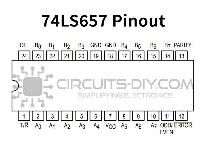
| Pin No. | Pin Name | Description |
|---|---|---|
| 1 | T/R’ | |
| 2 | A0 | A0 ports, 3–state inputs |
| 3 | A1 | A1 port, 3–state inputs |
| 4 | A2 | A2 port, 3–state inputs |
| 5 | A3 | A3 port, 3–state inputs |
| 6 | A4 | A4 port, 3–state inputs |
| 7 | VCC | Chip Supply Voltage |
| 8 | A5 | A5 port, 3–state inputs |
| 9 | A6 | A6 port, 3–state inputs |
| 10 | A7 | A7 port, 3–state inputs |
| 11 | ODD/EVEN’ | Parity select input |
| 12 | ERROR’ | Error output |
| 13 | PARITY | Parity output |
| 14 | B7 | B7 port, 3–state inputs |
| 15 | B6 | B6 port, 3–state inputs |
| 16 | B5 | B5 port, 3–state inputs |
| 17 | B4 | B4 port, 3–state inputs |
| 18 | GND | Ground Pin |
| 19 | GND | Ground Pin |
| 20 | B3 | B3 port, 3–state inputs |
| 21 | B2 | B2 port, 3–state inputs |
| 22 | B1 | B1 port, 3–state inputs |
| 23 | B0 | B0 port, 3–state inputs |
| 24 | OE’ | Output enable input (active low) |
Applications
the 74F657 has a wide array of applications, a few of them are mentioned as following
- Ideal in places where high output drive and light bus loading is required.
- Suitable for use in automotive applications.
74F657 Datasheet
You can download the datasheet for 74F657 Octal Bus Transceiver from the link given below:
See Also: 74LS138 1-To-8 Decoder/Demultiplexer IC – Datasheet | 74LS45 BCD to Decimal Decoders/Drivers IC – Datasheet | 74LS31 Hex Delay Element/Delay Line Generator IC – Datasheet