

Contents
hide
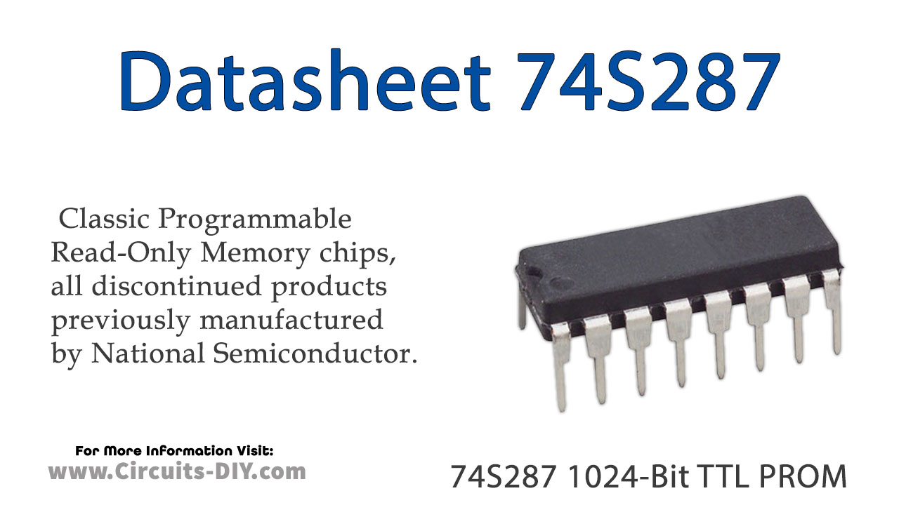
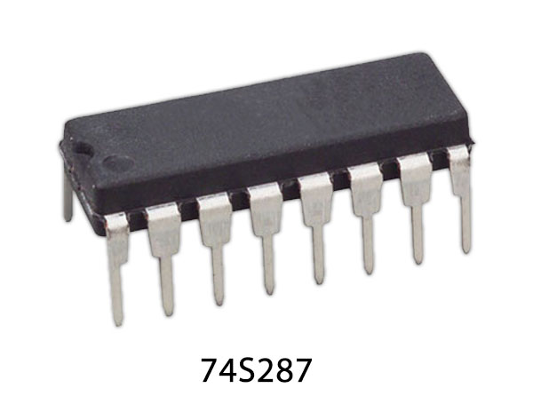
This Schottky memory is organized in the popular 32 words by 8 bits configuration. A memory enables input is provided to control the output states. When the device is enabled, the outputs represent the contents of the selected word. When disabled, the 8 outputs go to the “OFF” or high impedance state PROMs are shipped from the factory with lows in all locations. A high may be programmed into any selected location by following the programming instructions.
74S287 Pinout
74S287 Pin Configuration
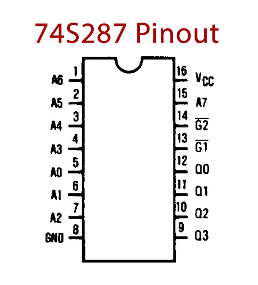
| Pin No | Pin Name | Description |
|---|---|---|
| 1 | A6 | Address Pin |
| 2 | A5 | Address Pin |
| 3 | A4 | Address Pin |
| 4 | A3 | Address Pin |
| 5 | A0 | Address Pin |
| 6 | A1 | Address Pin |
| 7 | A0 | Address Pin |
| 8 | GND | Ground Pin |
| 9 | Q3 | Data Output |
| 10 | Q2 | Data Output |
| 11 | Q1 | Data Output |
| 12 | Q0 | Data Output |
| 13 | G1′ | Output Enable |
| 14 | G2′ | Output Enable |
| 15 | A7 | Address Pin |
| 16 | VCC | Power Supply Pin |
74S287 Key Features
- Advanced titanium-tungsten (T-W) fuses
- Schottky-clamped for high speed
- Address access down to-25 ns max
- Enable access-20 ns max
- Enable recovery-20 ns max
- PNP inputs for reduced input loading
- All DC and AC parameters guaranted over temperature
- Low voltage TRI-SAFE programming
- TRI-STATE” Outputs
You can download this datasheet for 74S287 1024-Bit TTL PROM – Datasheet from the link given below:
Related posts:
 2N5322 PNP Small Signal Transistor - Datasheet
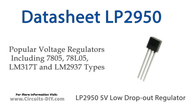 LP2950 5V 100mA Low Drop-out Regulator - Datasheet
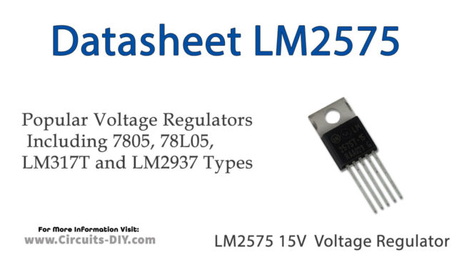 LM2575 15V 1A Step-Down Voltage Regulator - Datasheet
 2SB647 PNP General Purpose Transistor - Datasheet
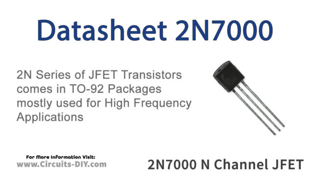 2N7000 0.2A 60V N-Channel Enhancement FET - Datasheet
 MJ1000 NPN Darlington Power Transistor - Datasheet