Contents
hide
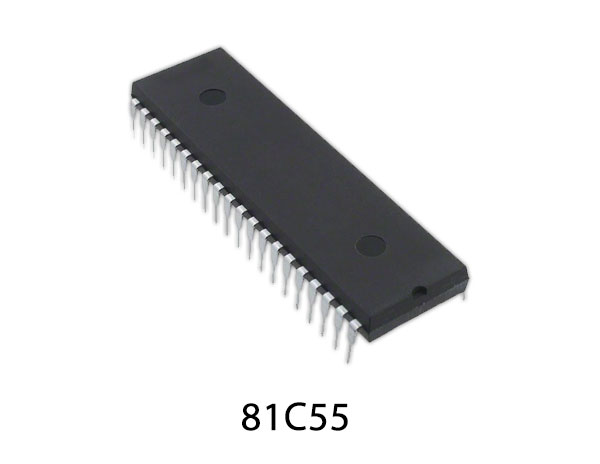
The 81C55 has 2k-bit static RAM (256 bytes) with parallel I/O ports and a timer. It uses silicon gate CMOS technology and consumes a standby current of 100 microamperes, maximum, while the chip is not selected. Featuring a maximum access time of 400 ns, the 81C55 can be used in an 80C85 system without using wait states.
The parallel I/O consists of two 8-bit ports and one 6-bit port (both general purpose). The 81C55 also contains a 14-bit programmable counter/timer which may be used for sequence-wave generation or terminal count-pulsing.

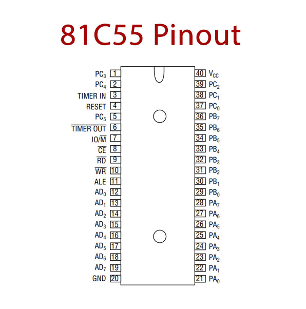
81C55 Pinout

81C55 Pin Configuration
| Pin Number | Pin Name | Description |
|---|---|---|
| 1 | PC3 | Port C |
| 2 | PC4 | Port C |
| 3 | TIMER IN | Timer Input |
| 4 | RESET | Reset |
| 5 | PC5 | Port C |
| 6 | TIMER OUT | Timer Output (Active Low) |
| 7 | IO/M | Internal Memory Select |
| 8 | CE | Chip Enable (Active Low) |
| 9 | RD | Read (Active Low) |
| 10 | WR | Write (Active Low) |
| 11 | ALE | Address Latch Enable |
| 12-19 | AD0-AD7 | Address Data Bus |
| 20 | GND | Ground |
| 21-28 | PA0-PA7 | Port A |
| 29-36 | PB0-PB7 | Port B |
| 37-39 | PC0-PC2 | Port C |
| 40 | Vcc | Positive Voltage Supply |
81C55 Key Features
- High speed and low power achieved with silicon gate CMOS technology
- 256 words x 8bits RAM
- Single power supply, 3 to 6 V
- Completely static operation
- On-chip address latch
- 8-bit programmable I/O ports (port A and B)
- TTL Compatible
- RAM data hold characteristic at 2 V
- 6-bit programmable I/O port (port C)
- 14-bit programmable binary counter/timer
- Multiplexed address/data bus
You can download this datasheet for 81C55 RAM I/O Port Timer – Datasheet from the link given below:


