
The CD4044 IC consists of four R-S latches, made by using the NAND logical gate. There is a common 3-STATE ENABLE input for all four latches. A logic “1” on the ENABLE input connects the latch states to the Q outputs. A logic “0” on the ENABLE input disconnects the latch states from the Q outputs resulting in an open circuit condition on the Q output. The 3-STATE feature allows the common bussing of the outputs. The IC has many features such as high noise immunity, ESD barring, and excellent thermal overload protection.
What is an R-S Latch?
An SR latch or an SR Flip-Flop is a combinational logic circuit, that has two inputs S and R, and two outputs Q and Q’. The state of this latch is determined by the condition of output Q. If output Q is 1 (High) the latch is said to be SET and if Q is 0 (Low) the latch is said to be RESET. An SR Latch or Flip flop can be designed either by two cross-coupled NAND gates or two-cross coupled NOR gates.
CD4044 Key Features
- Wide supply voltage range: 3V to 15V
- Low power: 100 nW (typ.)
- High noise immunity: 0.45 VDD (typ.)
- Separate SET and RESET inputs for each latch
- NOR and NAND configuration
- 3-STATE output with common output enable
CD4044 Pinout
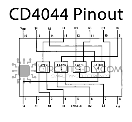
| Pin No | Pin Name | Description |
|---|---|---|
| 1 | Q4 | output latch 4 |
| 2 | NC | no connection |
| 3 | S1 | set input for latch 1 |
| 4 | R1 | reset input for latch 1 |
| 5 | ENB | enable input |
| 6 | R2 | reset input for latch 2 |
| 7 | S2 | set input for latch 2 |
| 8 | VSS | source supply |
| 9 | Q2 | output latch 2 |
| 10 | Q3 | output latch 3 |
| 11 | S3 | set input for latch 3 |
| 12 | R3 | reset input for latch 3 |
| 13 | Q1 | output latch 1 |
| 14 | R4 | reset input for latch 4 |
| 15 | S4 | set input for latch 4 |
| 16 | VDD | Drain supply |
Application
- Multiple bus storage
- Strobed register
- Four bits of independent storage with output enable
- General digital logic
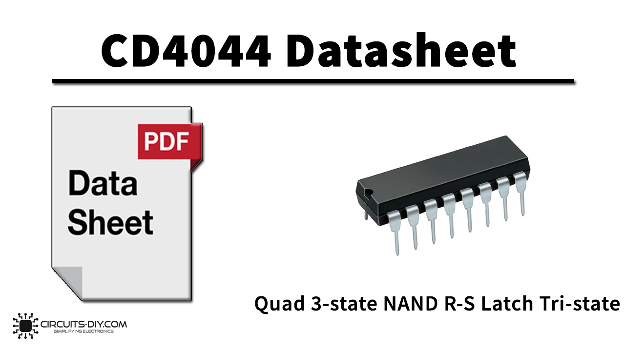
CD4044 Datasheet
You can download the datasheet for CD4044 Quad 3-state NAND R-S Latch with Tristate outputs from the link given below:
See Also: CD4516 Binary Up Down Counter – Datasheet | CD4007 Dual Complementary Pair with Inverter – Datasheet | CD4094 8-stage Shift-and-Store Bus Register – Datasheet
Related posts:
 74LS07 Hex Buffer with High Voltage Open-Collector Outputs - Datasheet
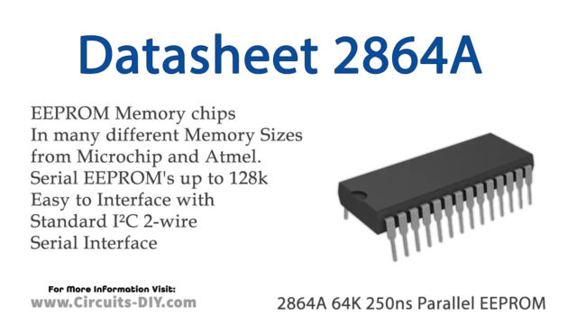 2864A 64K 250ns Parallel EEPROM - Datasheet
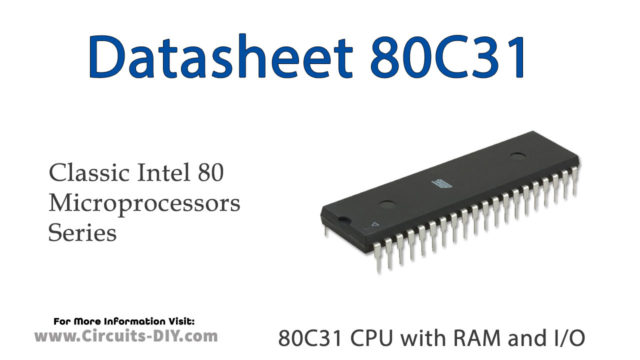 80C31 CPU with 128x8 RAM and I/O - Datasheet
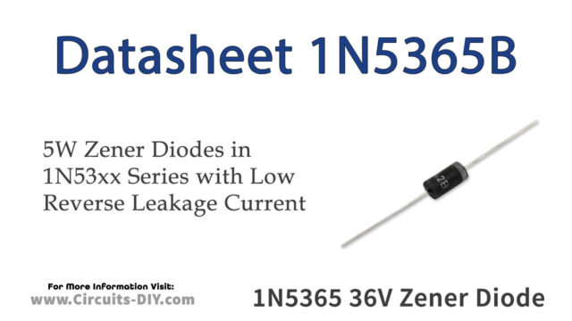 1N5365B 36V 5W Zener Diode - Datasheet
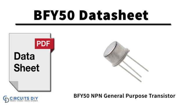 BFY50 NPN General Purpose Transistor - Datasheet
 CD4098 CMOS/MOS Dual Mono-stable Multvibrator - Datasheet


