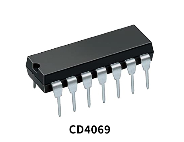
The CD4069 consists of six inverter circuits and is manufactured using complementary MOS (CMOS) to achieve wide power supply operating range, low power consumption, high noise immunity, and symmetric controlled rise and fall times. This device is intended for all general purpose inverter applications where the special characteristics of the MM74C901, MM74C907, and CD4049 Hex Inverter/Buffers are not required. In those applications requiring larger noise immunity the MM74C14 or MM74C914 Hex Schmitt Trigger is suggested. All inputs are protected from damage due to static discharge by diode clamps to VDD and VSS
What is a Hex Inverter?
A hex inverter is a simple digital logic circuit that can generate logical inverse any input signal. The output of a hex inverter is always high (1) when the input signal is low (0). Similarly, a hex inverter always yields a low (0) output when the input signal is high (1).
CD4069 Key Features
- Wide supply voltage range: 3.0V to 15V
- High noise immunity: 0.45 VDD typ.
- Low power TTL compatibility: Fan out of 2 driving 74L
- or 1 driving 74LS
- Equivalent to MM74C04
CD4069 Pinout
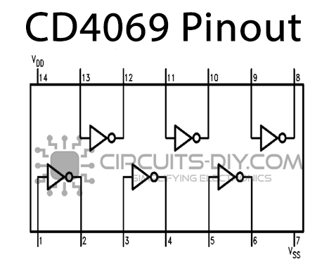
| Pin No | Pin Name | Description |
|---|---|---|
| 1 | A | input of inverter A |
| 2 | A’ | inverted output of A |
| 3 | B | input of inverter B |
| 4 | B’ | inverted output of B |
| 5 | C | input of inverter C |
| 6 | C’ | inverted output of C |
| 7 | VSS | source supply |
| 8 | D’ | inverted output of D |
| 9 | D | input of inverter D |
| 10 | E’ | inverted output of E |
| 11 | E | input of inverter E |
| 12 | F’ | inverted output of F |
| 13 | F | input of inverter F |
| 14 | VDD | Drain supply |
Application
- Logic inversion
- Pulse shaping
- Oscillators
- High-input-impedance amplifiers
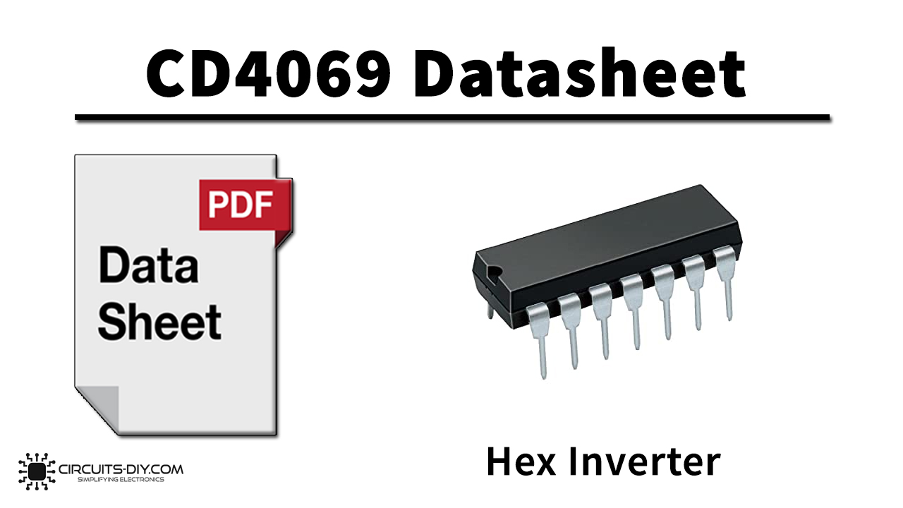
CD4069 Datasheet
You can download the datasheet for CD4069 Hex Inverter IC from the link given below:
See Also: CD40110 Decade Up/Down Counter – Datasheet | CD4585 4-bit Comparator – Datasheet | CD4543 BCD to 7-Segment Decoder – Datasheet