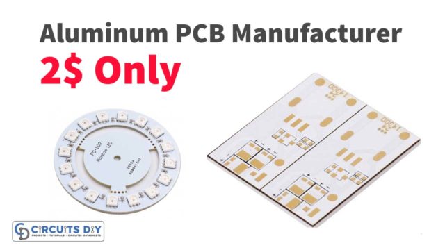
In the modern world, electronic and digital devices are becoming the basic needs of customers, organizations, and industries. The printed circuit boards are the main components of the devices that direct the electrical signals in them. Some of the less complex devices may require simple or generic boards while other devices that have complex structures may require custom PCB assembly.
Some customers may want to assemble the PCB according to the specific requirements and design. This process is referred to as the manufacturing of custom PCB. The process of making a custom PCB is quite similar to the basic process which involves transforming the schematic design into the physical board, selection of the materials, fabrication, and then the assembly of the board.
In the custom PCB assembly process, the components such as transformers, diodes, transmitters, capacitors, resistors, and ICs are mounted on the board according to the required design and customer requirement which makes it fully functional. PCB fabrication and PCB assembly is the most fundamental components in making devices compact, efficient, and of better quality. Following are the few steps in manufacturing a custom PCB board.
This article will provide you with all the information that you may need in manufacturing a complete custom PCB assembly, from PCB design and layout, to PCB assembly and final inspection.
Schematic View
If a customer wants a custom PCB board then the manufacturer will ask about the requirement and what type of design he needs. The manufacturer will use the advanced software to make a blueprint or schematic view of the PCB assembly according to the requirement.
The blueprint will identify the required components and connections within the circuit board. In the schematic view, the packages like inline or surface mount may seem similar but they are very different while designing the layout of the board.
Layout Design
In the next step of custom PCB assembly, the layout design of the board will be generated which includes the placement and tracing of the components like copper. They are arranged in an ideal pattern and it is also made sure that the footprints of the components would fit in the PCB assembly.
Layout design could also be custom and once the design is approved by the customer it can be sent to the next step which is to make the Gerber files that are used in the PCB fabrication. Each PCB board has many files depending on the layers and each layer has one file on it, besides copper layers, there are solder mask layers, silkscreen layers, and drill layers.
Bill of Materials
It contains all the components that are needed to be mounted on the boards. When the design is approved the final bill of materials is confirmed. It may have the number and quantity of each component, specifications, part numbers, and the locations of the components. Generally speaking, a bill of materials (BOM) tells us which components should be used, and where they should be soldered.
Prototyping
Next comes the prototyping of the custom PCB. It can be simple or complex depending on the demand and requirement of the customer. Gerber files are used to make both simple and complex PCB prototypes. In simple designs, there are only one or two layers of the board and it is without the attachment of too many electronic components. On the other hand, the complex designs may have multilayered boards and may also require additional layers or drills.
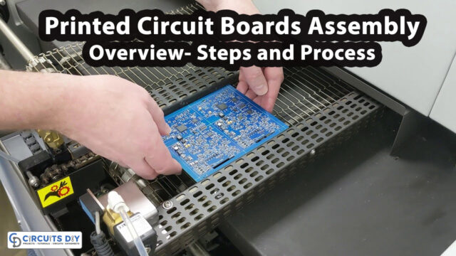
Next, to assemble the components on boards it is made sure that the manufacturers have all the desired materials mentioned in the BOM and then it is approved by the customer for custom PCB assembly. It is done with the combination of both manual and automatic processes to approve the final design of custom PCB assembly. The soldering may be done by hand, by using surface mount technology through-hole technology, and wave soldering. After the prototype is made, it is then tested by the engineers in the lab. If it is not perfect then the team would have to optimize the design again to make the custom PCB.
If the board has components like microcontrollers and FPGAs, the firmware would be uploaded on the prototype but it will depend on the customer’s need. If he doesn’t want the firmware then this step can be skipped.
Custom PCB Fabrication
If the customer PCB prototypes pass the final test, then it is time to start real mass production. Before starting a custom PCB assembly, we need to produce the printed circuit boards first. PCB production is a very complex step, the process includes pattern imaging and development, etching, drilling, plating, solder mask and silkscreen printing, surface treatment, testing, and inspections. Complex circuit boards like HDI PCB and rigid-flex PCB will need several extra steps. So a reliable PCB manufacturer is quite important to get your circuit boards done in good quality.
PCBs can be categorized into layers, material, technology, usage., etc. According to to layers, there are single-layer PCBs, double-layer PCBs, and multilayer PCBs. According to materials, there are FR-4 PCBs, CEM-1/CEM3 PCBs, high TG PCBs, high-speed PCBs, high-frequency PCBs, ceramic PCBs, PTFE PCBs, Teflon PCBs, polyimide PCBs., etc. According to technology, there are HDI PCBs, impedance PCBs, gold connector PCBs, microvia PCBs, backplane PCBs., etc. According to the usage, there are circuit boards for industrial, consumer, automotive, medical, telecommunications, and aerospace., etc.
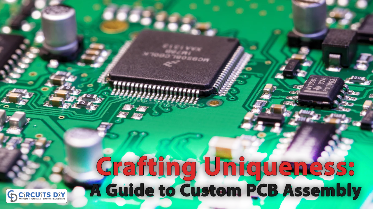
Custom PCB Assembly
When the design and prototype are approved by the customer and after having all the materials including PCB bare boards, the manufacturer moves towards the main process which is the custom PCB board assembly. The assembly can be done with the help of different machines like the automated solder paste machine, SMT pick and place machine, and wave solder machine.
They are used for different purposes like to do the groundwork of substrate with the help of a printer, the automated solder paste machine is used, for the assignment of materials, pick and place machine, and sealing the connection after soldering, the wave soldering machine is used.
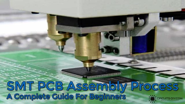
For the custom PCB assembly, the soldering can be done through both SMT & THT technologies. However, it depends on the design of the custom PCB board. For the high-density circuits, the SMT is appropriate relative to the THT.
If you are using the through-hole technology the process is simple and you have to go through a few steps like attachment of components to PCB, wave soldering machine to make the connection between the materials, heat curing, and washing of optional custom PCB.
However, if you are using the SMT for the custom PCB assembly, the procedure could be complex. First, the printer is used to apply the solder paste and attach the components with the help of the pick and place machine, then there is reflow soldering, flipping of custom PCB to apply the solder paste on the other side and if there are any additional components they are also surface mounted on the custom circuit board assembly and through-hole components are added if required.
As discussed earlier if there is a requirement of firmware, then it is installed exactly where it needs to be as per the design of the custom PCB board.
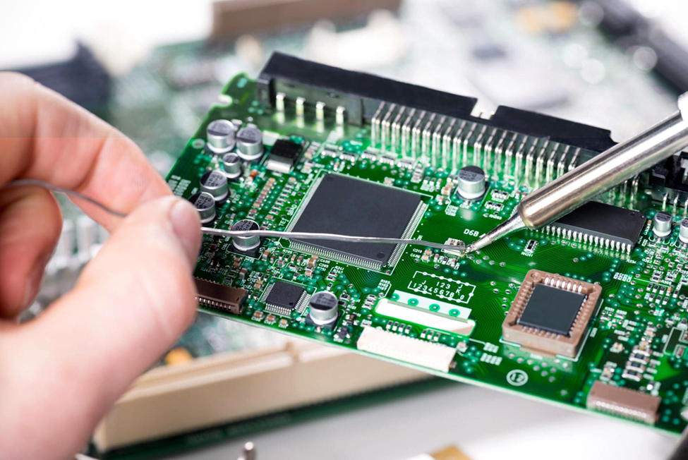
Inspection of Custom PCB
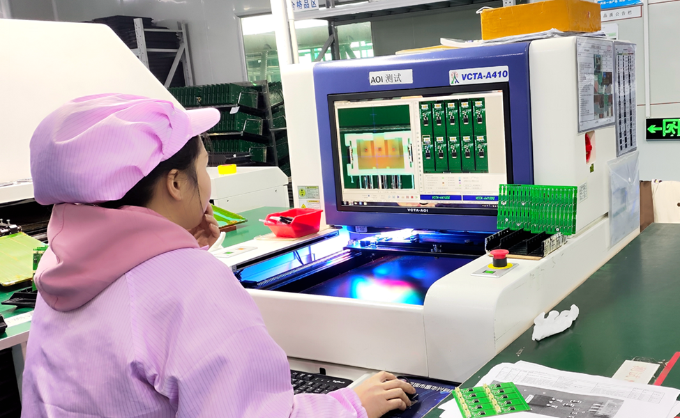
To detect any errors in the PCB assembly and to check the quality of the custom PCB boards, the manufacturers undergo the quality control process. It can be done by visual inspection, automated visual inspection or by x-ray mechanism. AOI uses the cameras to detect any faults in the PCB boards. In-circuit tests also help to check and test if the components are soldered correctly.
The final step in the custom PCB assembly is to test the functionality of the board. For this purpose, the electrical test is used to verify that the custom PCB board is functioning properly and no defaults are recorded.
If any abnormality is recorded the board has to go through all the custom PCB assembly processes or otherwise, the assembly would be discarded or re-worked.
Conclusion
Electronic and digital devices with optimal performance, dependability, and manufacturability can be created readily now, thanks to custom PCB assembly technology. Now with the help of an advanced PCB assembly process and with careful planning and production, a more complex custom PCB can be created that can fulfill the needs of the customer, organizations, and industries.