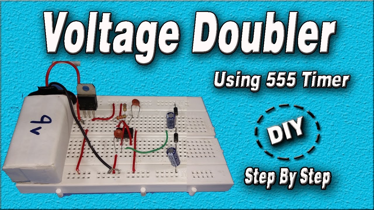
What is a Voltage Doubler?
The Voltage Doubler is the circuit where we get twice 2x of the input voltage if we supply 5v, we will get 10 volts at the output. Generally, transformers are there to step-up or step-down the voltage, but sometimes transformers are not feasible because of their size and cost. So in this tutorial, we are going to make a “Voltage Doubler Circuit using 555 Timer IC”
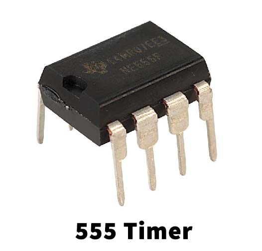
The heart of this circuit is a NE555 Timer IC. The IC possesses an oscillation frequency ranging from 670 to 680 Hz. Here, this NE555 timer acts as an astable multivibrator An astable multivibrator is a free-running oscillator that switches continuously between its two unstable states. With no external signal applied, the transistors alternately switch from cutoff to saturation state at a frequency that RC time constants of the coupling circuit determine. If these time constants are equal (R and C are equal) then a square wave will generate with a frequency of 1/1.4 RxC. Hence, an astable multivibrator is also a pulse generator or a square wave generator.
Hardware Components
The following components are required to make the Voltage Doubler Circuit
| S.No | Component | Value | Qty |
|---|---|---|---|
| 1. | Breadboard | – | 1 |
| 2. | DC Supply | 12v | 1 |
| 3. | Connecting wires | – | 1 |
| 4. | IC | NE555 Timer | 1 |
| 5. | Regulator IC | LM7805 | 1 |
| 6. | Diode | 1N4007 | 2 |
| 7. | Resistors | 10k, 33k | 1, 1 |
| 8. | Ceramic Capacitor | 22uF, 0.01uF, 0.1uF | 2, 1, 1 |
555 IC Pinout
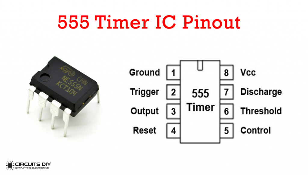
For a detailed description of pinout, dimension features, and specifications download the datasheet of 555 Timer
7805 Pinout
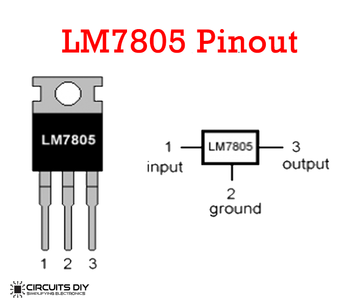
For a detailed description of pinout, dimension features, and specifications download the datasheet of LM705
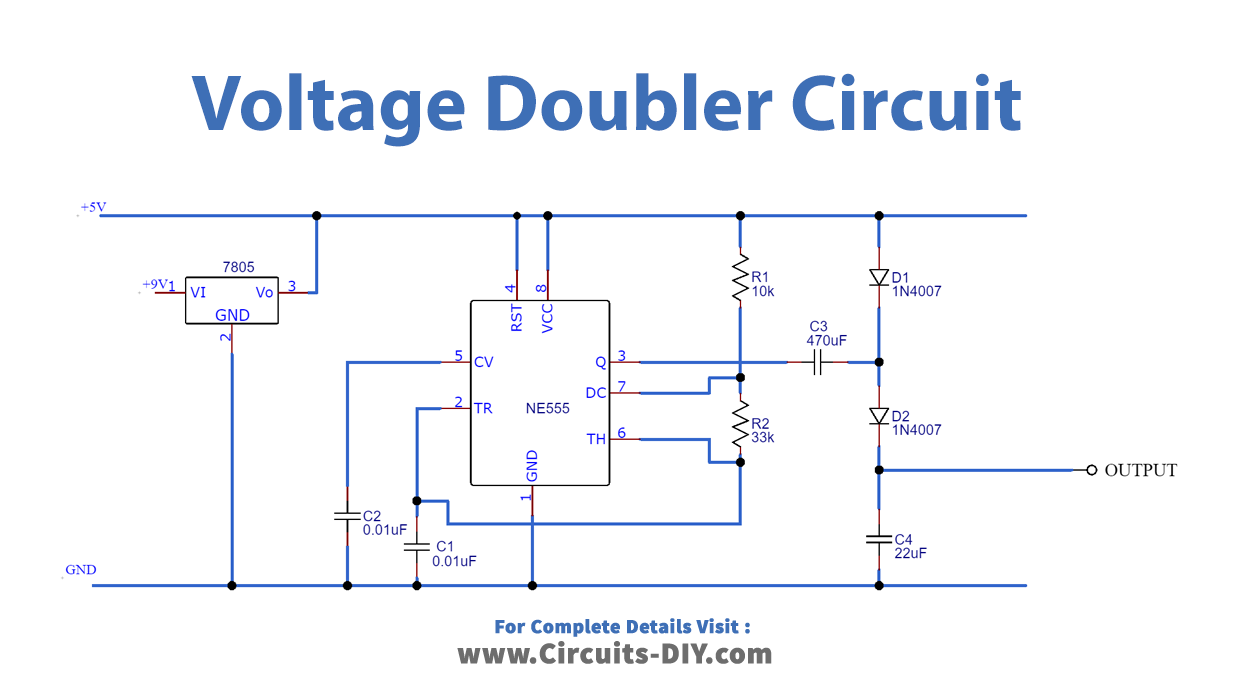
Voltage Doubler Circuit
Working Explanation
The working of this circuit can be broken down into two parts. The first part consists of the 555 timer IC in Astable mode, which generates the square wave and the second part consists of diodes (D1 & D2) and 2 capacitors (C3 & C4) to double the output voltage.
When the output at OUT Pin of NE555 IC is low, diode D1 gets forward biased and capacitor C3 gets charged through the diode D1. Capacitor C3 (22uF) gets charged up to the same voltage as the source, which is 5V in our case. Now when output at Pin 3 (OUT) goes high, D1 gets reverse biased and blocks the discharging of the capacitor C3, and at the same time, D2 is forward biased and allows the capacitor C4 to charge. Now the capacitor C4 (22uF) charges with the combined voltage of Capacitor C3 and the input source voltage, which means 5V of capacitor C3 and 5V of input supply, so it charges up to approximately 10V, Hence doubling the output voltage.
Applications
- They serve in many electrical and electronic applications such as microwave ovens, strong electric field coils for cathode-ray tubes, electrostatic and high voltage test equipment, etc.