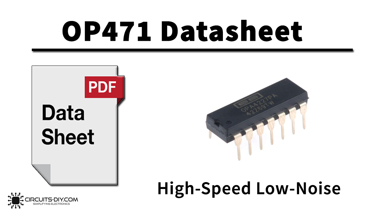
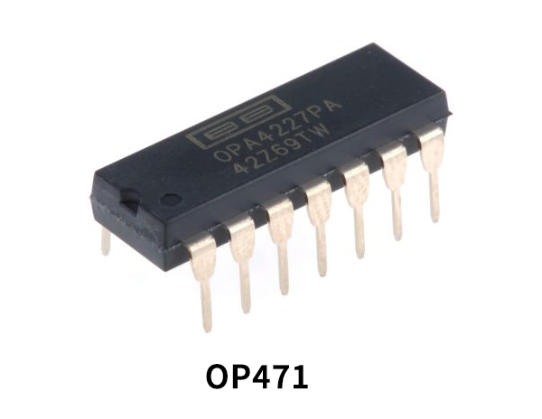
OP471 is a High-Speed Low-Noise Quad Op-Amp IC. OP471 has an input offset voltage under 0.8 mV and input offset voltage drift below 4 mV/∞C, guaranteed over the full military temperature range. The open-loop gain of the OP471 is over 500,000 into a 10 kW load ensuring outstanding gain accuracy and linearity.
Operational Amplifier
An operational amplifier is one of the basic building blocks for analog circuits, An operational amplifier takes in differential voltage input and produces a single-ended voltage output. The basic purpose of employing an operational amplifier in an analog circuit is to perform the function of signal amplification: The process of boosting an electrical signal of low strength to a level of higher amplitude. Op-amps also function as a filter of the input signal; meaning that, an operational amplifier is able to extract the signal with the target frequency. Op-amps can be divided into two fundamental parts:
- Precision Op-amps
- Differential Op-amps
OP471 Pinout
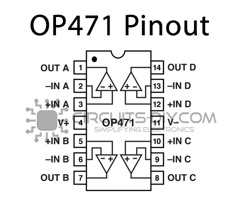
OP471 Pin Configuration
| Pin No | Pin Name | Description |
|---|---|---|
| 1 | OUT A | Output Of Amplifier A |
| 2 | INV-INPUT A | Inverting Input Of Amplifier A |
| 3 | NON-INV-INPUT A | Non Inverting Input Of Amplifier A |
| 4 | V+ | Positive Power Supply |
| 5 | NON-INV-INPUT B | Non Inverting Input Of Amplifier B |
| 6 | INV-INPUT B | Inverting Input Of Amplifier B |
| 7 | OUT B | Output Of Amplifier B |
| 8 | OUT C | Output Of Amplifier C |
| 9 | INV-INPUT C | Inverting Input Of Amplifier C |
| 10 | NON-INV-INPUT C | Non Inverting Input Of Amplifier C |
| 11 | V- | Negative Power Supply |
| 12 | NON-INV-INPUT D | Non Inverting Input Of Amplifier D |
| 13 | INV-INPUT D | Inverting Input Of Amplifier D |
| 14 | OUT D | Output Of Amplifier D |
OP471 Features
- Excellent Speed: 8 V/s Typ
- Low Noise: 11 nV/˜Hz @ 1 kHz Max
- Unity-Gain Stable
- High Gain Bandwidth: 6.5 MHz Typ
- Low Input Offset Voltage: 0.8 mV Max
- Low Offset Voltage Drift: 4 V/C Max
- High Gain: 500 V/mV Min
- Outstanding CMR: 105 dB Min
Application
- Low Noise Amplifier
A simple method of reducing amplifier noise by paralleling amplifiers is shown in Figure 13. Amplifier noise, depicted in Figure 14, is around 5 nV/˜Hz @ 1 kHz (R.T.I.). Gain for each paralleled amplifier and the entire circuit is 100. The 200 W resistors limit circulating currents and provide an effective output resistance of 50 W. The amplifier is stable with a 10 nF capacitive load and can supply up to 30 mA of output drive.
OP471 Datasheet
You can download this datasheet for OP471 High-Speed Low-Noise Quad Op-Amp from the link given below:
See Also: CD4052 Differential 4-channel Multiplexer/Demultiplexer Datasheet | CD4066 Quad Bilateral Switch – Datasheet | CD4030 Quad EXCLUSIVE-OR Gate -Datasheet