
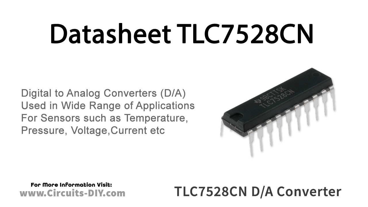
The TLC7528CN is dual, 8-bit, digital-to-analog converters designed with separate on-chip data latches and feature exceptionally close DAC-to-DAC matching. Data is transferred to either of the two DAC data latches through a common, 8-bit, input port. Control input DACA/DACB determines which DAC is to be loaded. The load cycle of these devices is similar to the write cycle of a random-access memory, allowing easy interface to most popular microprocessor buses and output ports. Segmenting the high-order bits minimizes glitches during changes in the most significant bits, where glitch impulse is typically the strongest.
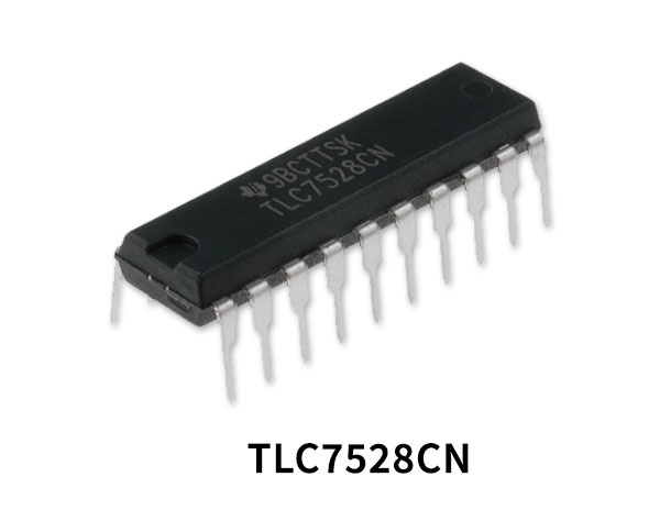
TLC7528CN Pinout
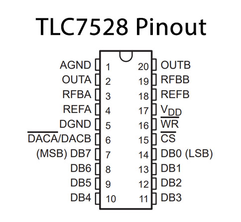
TLC7528CN Pin Configuration
| Pin No | Pin Name | Description |
|---|---|---|
| 1 | AGND | Analog Ground |
| 2 | OUTA | DACA output |
| 3 | RFBA | ±10V Range Feedback Output A |
| 4 | REFA | Voltage reference input A |
| 5 | DGND | Digital Ground |
| 6 | DACA’/DACB | DACA output (Active Low) /DACB output |
| 7 | DB7 (MSB) | Digital DAC data input DB7 |
| 8 | DB6 | Digital DAC data input DB6 |
| 9 | DB5 | Digital DAC data input DB5 |
| 10 | DB4 | Digital DAC data input DB4 |
| 11 | DB3 | Digital DAC data input DB3 |
| 12 | DB2 | Digital DAC data input DB2 |
| 13 | DB1 | Digital DAC data input DB1 |
| 14 | DB0 (LSB) | Digital DAC data input DB0 |
| 15 | CS’ | Chip Select (Active Low) |
| 16 | WR’ | Write input (Active Low) |
| 17 | VDD | Positive supply voltage input terminal |
| 18 | REFB | Voltage reference input B |
| 19 | RFBB | ±10V Range Feedback Output B |
| 20 | OUTB | DACB output |
TLC7528CN Features
- Easily Interfaced to Microprocessors
- On-Chip Data Latches
- Monotonic Over the Entire A/D Conversion Range
- Interchangeable With Analog Devices AD7528 and PMI PM-7528
- Fast Control Signaling for Digital Signal Processor (DSP) Applications Including Interface With TMS320
- Voltage-Mode Operation
- CMOS Technology
TLC7528CN Specification
- Resolution 8 bits
- Linearity Error 1/2 LSB
- Power Dissipation at VDD = 5 V 20 mW
- Settling Time at VDD = 5 V 100 ns
- Propagation Delay Time at VDD = 5 V 80 ns
Application
- Microprocessor-controlled gain-setting
- Signal-control application
You can download this datasheet for TLC7528CN Dual 8-bit Multiplying D/A Converter from the link given below: