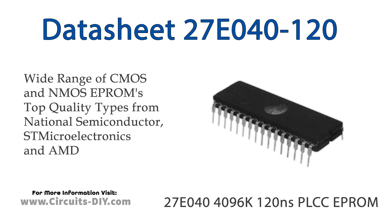
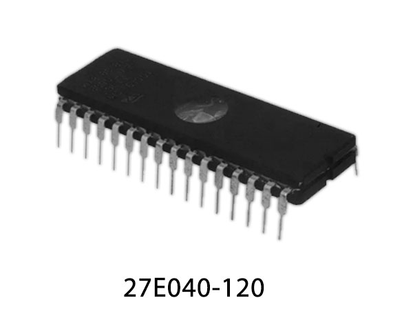
The W27E040 is a high-speed, low-power Electrically Erasable and Programmable Read-Only Memory organized as 524288 ´ 8 bits that operate on a single 5-volt power supply. The W27E040 provides an electrical chip erase function
27E040 Pinout
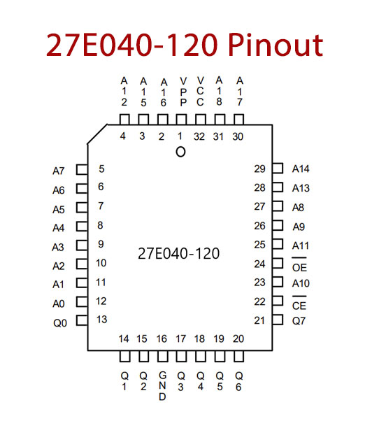
27E040 Pin Configuration
| Pin Number | Pin Name | Description |
|---|---|---|
| 1 | VPP | Programming Supply |
| 2 | A16 | Address Input 16 |
| 3 | A15 | Address Input 15 |
| 4 | A12 | Address Input 12 |
| 5 | A7 | Address Input 7 |
| 6 | A6 | Address Input 6 |
| 7 | A5 | Address Input 5 |
| 8 | A4 | Address Input 4 |
| 9 | A3 | Address Input 3 |
| 10 | A2 | Address Input 2 |
| 11 | A1 | Address Input 1 |
| 12 | A0 | Address Input 0 |
| 13 | Q0 | Data Input 0 |
| 14 | Q1 | Data Input 1 |
| 15 | Q2 | Data Input 2 |
| 16 | VSS | Ground Pin |
| 17 | Q3 | Data Input 3 |
| 18 | Q4 | Data Input 4 |
| 19 | Q5 | Data Input 5 |
| 20 | Q6 | Data Input 6 |
| 21 | Q7 | Data Input 7 |
| 22 | CE’ | Chip Enable |
| 23 | A10 | Address Input 10 |
| 24 | OE’ | Output Enable |
| 25 | A11 | Address Input 11 |
| 26 | A9 | Address Input 9 |
| 27 | A8 | Address Input 8 |
| 28 | A13 | Address Input 13 |
| 29 | A14 | Address Input 14 |
| 30 | A17 | Address Input A17 |
| 31 | A18 | Address Input A18 |
| 32 | Vcc | Positive Power Supply |
27E040 Key Features
- High-speed access time:
- 90/120 nS (max.)
- Read operating current: 15 mA (typ.)
- Erase/Programming operating current
- 15 mA (typ.)
- Standby current: 5 mA (typ.)
- Single 5V power supply
- +14V erase/+12V programming voltage
- Fully static operation
- All inputs and outputs directly TTL/CMOS compatible
You can download this datasheet for 27E040 4096K 120ns PLCC EPROM – Datasheet from the link given below: