
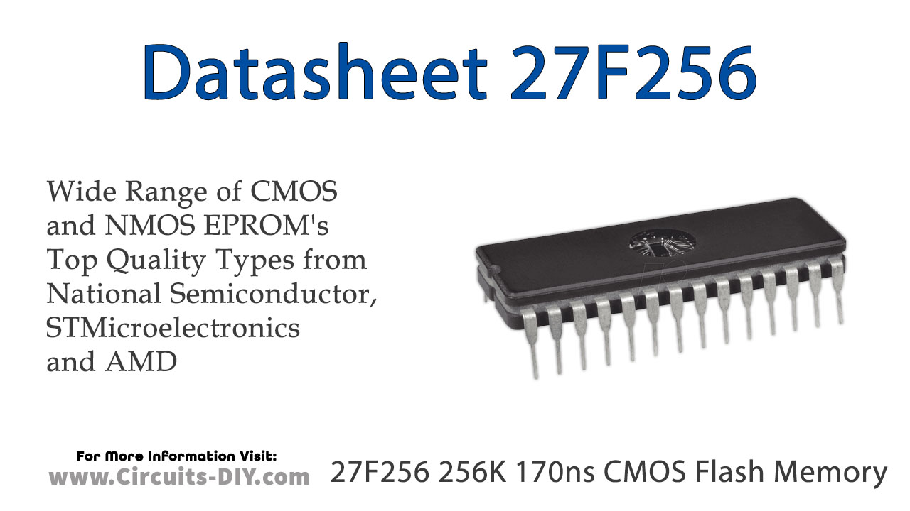
27F256 CMOS flash memory offers the most cost-effective and reliable alternative for updatable non-volatile memory. The 27F256 adds electrical chip-erasure and reprogramming to familiar EPROM technology. Memory contents can be erased and reprogrammed: in a test socket; in a PROM-programmer socket; onboard during subassembly test; in-system during the final test; and in-system after-sale. The 27F256 increases memory flexibility while contributing to time- and cost savings.
The 27F256 is targeted for alterable code or data-storage applications where EPROM ultraviolet erasure is impractical or time-consuming. The 27F256 can also be applied where traditional EEPROM functionality (byte-erasure) is either not required or not cost-effective. The 27F256 is a 256-kilobit nonvolatile memory organized as 32768 bytes of 8 bits. Intel’s 27F256 is offered in a 28-pin “windowless” credit package. Pin assignments conform to JEDEC standards for byte-wide EPROMs. Intel’s 27F256 employs advanced CMOS circuitry for systems requiring high-performance access speeds, low power consumption, and immunity to noise.
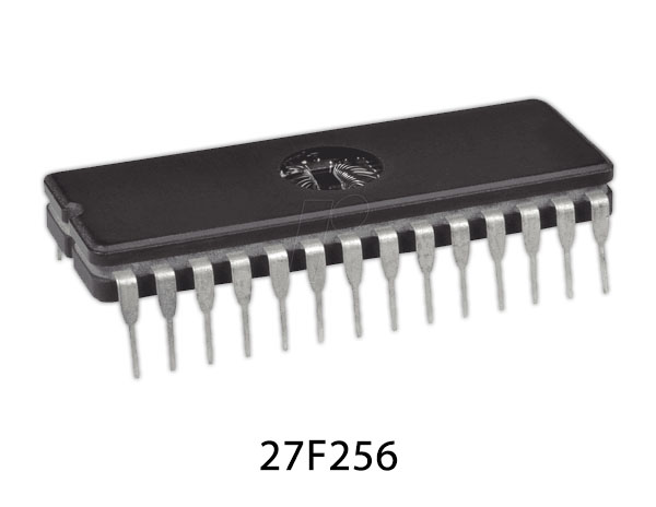
27F256 Pinout
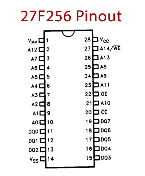
27F256 Pin Configuration
| Pin Number | Pin Name | Description |
|---|---|---|
| 1 | VPP | Programming Supply |
| 2 | A12 | Address Input |
| 3 | A7 | Address Input |
| 4 | A6 | Address Input |
| 5 | A5 | Address Input |
| 6 | A4 | Address Input |
| 7 | A3 | Address Input |
| 8 | A2 | Address Input |
| 9 | A1 | Address Input |
| 10 | A0 | Address Input |
| 11 | DQ0 | Data Output |
| 12 | DQ1 | Data Output |
| 13 | DQ2 | Data Output |
| 14 | VSS | Ground Pin |
| 15 | DQ3 | Data Output |
| 16 | DQ4 | Data Output |
| 17 | DQ5 | Data Output |
| 18 | DQ6 | Data Output |
| 19 | DQ7 | Data Output |
| 20 | CE’ | Chip Enable |
| 21 | A10 | Address Input |
| 22 | OE | Output Enable |
| 23 | A11 | Address Input |
| 24 | A9 | Address Input |
| 25 | A8 | Address Input |
| 26 | A13 | Address Input |
| 27 | A14 | Address Input |
| 28 | Vcc | Positive Power Supply |
27F256 Key Features
- Flash Electrical Chip-Erase
- 1 Second Typical Chip-Erase
- Quick-Pulse ProgrammingTM
- 100 us Typical Byte-Program
- 4 Second Chip-Program
- EPROM-Compatible 12.75V Vpp Supply
- 100 Erase/Program Cycles Minimum
- High-Performance Speeds
- 170 ns Maximum Access Time
- Low Power Consumption
- 100 A Maximum Standby Current
You can download this datasheet for 27F256 256K 170ns CMOS Flash Memory – Datasheet from the link given below: