
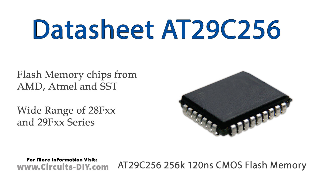
The 29C256 is a five-volt-only in-system Flash programmable and erasable read-only memory (PEROM). Its 256K of memory is organized as 32,768 words by 8 bits. The device offers access times to 70 ns with a power dissipation of just 275 mW. When the device is deselected, the CMOS standby current is less than 300 µA. Five-volt-only commands determine the operation of the device. Reading data out of the device is similar to reading from a static RAM. Reprogramming the AT29C256 is performed on a page basis; 64 bytes of data are loaded into the device and then simultaneously programmed. The contents of the entire device may be erased by using a six-byte software code (although erasure before programming is not needed)
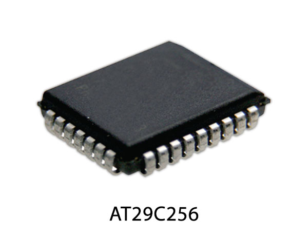
29C256 Pinout
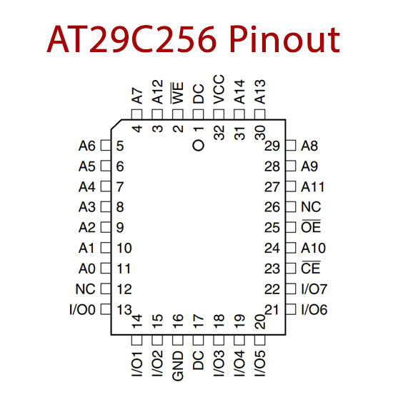
29C256 Pin Configuration
| Pin No | Pin Name | Description |
|---|---|---|
| 1 | DC | Don’t Connect |
| 2 | WE’ | Write Enable Pin |
| 3 | A12 | Address Pin 12 |
| 4 | A7 | Address Pin 7 |
| 5 | A6 | Address Pin 6 |
| 6 | A5 | Address Pin 5 |
| 7 | A4 | Address Pin 4 |
| 8 | A3 | Address Pin 3 |
| 9 | A2 | Address Pin 2 |
| 10 | A1 | Address Pin 1 |
| 11 | A0 | Address Pin 0 |
| 12 | NC | No Connection |
| 13 | I/O 0 | Data Inputs/Outputs 0 |
| 14 | I/O 1 | Data Inputs/Outputs 1 |
| 15 | I/O 2 | Data Inputs/Outputs 2 |
| 16 | GND | Ground Pin |
| 17 | DC | Don’t Connect |
| 18 | I/O 3 | Data Inputs/Outputs 3 |
| 19 | I/O 4 | Data Inputs/Outputs 4 |
| 20 | I/O 5 | Data Inputs/Outputs 5 |
| 21 | I/O 6 | Data Inputs/Outputs 6 |
| 22 | I/O 7 | Data Inputs/Outputs 7 |
| 23 | CE’ | Chip Enable Pin |
| 24 | A10 | Address Pin 10 |
| 25 | OE’ | Output Enable Pin |
| 26 | NC | No Connection |
| 27 | A11 | Address Pin 11 |
| 28 | A9 | Address Pin 9 |
| 29 | A8 | Address Pin 8 |
| 30 | A13 | Address Pin 13 |
| 31 | A14 | Address Pin 14 |
| 32 | VCC | Power Supply |
29C256 Key Feature
- Fast Read Access Time – 70 ns
- 5-Volt-Only Reprogramming
- Sector Program Operation
- Single Cycle Reprogram (Erase and Program)
- Internal Address and Data Latches for 64-Bytes
- Internal Program Control and Timer
- Hardware and Software Data Protection
- Two 16 KB Boot Blocks with Lockout
- Fast Sector Program Cycle
- Page (64 Byte) Program Time – 10 ms
- Chip Erase Time – 10 ms
- DATA Polling for End of Program Detection
- Low Power Dissipation
- 50 mA Active Current
- 300 µA CMOS Standby Current
- Typical Endurance > 10,000 Cycles
- Single 5V ± 10% Supply
- CMOS and TTL Compatible Inputs and Outputs
You can download this datasheet for 29C256 256k 120ns CMOS Flash Memory – Datasheet from the link given below: