The 74F543 is a part of the high speed 74F family. 74F543 octal registered transceiver contains two sets of D-type latches for the temporary storage of data flowing in either direction. Separate Latch Enable and Output Enable inputs are provided for each register to permit independent control of inputting and outputting in either direction of data flow. The A outputs are guaranteed to sink 24 mA while the B outputs are rated for 64 mA. The 74F543 IC has a vast array of working voltage, a wide range of working conditions, and directly interfaces with CMOS, NMOS, and TTL.
What is a Bus Transceiver?
Bus transceivers are electronic tri-state, bi-directional devices that allow the flow of data between two points, making them compatible with bus-oriented systems or the bi-directional (input or output) control of any interface circuitry. A Bus transceiver can be inverting or non-inverting, common examples are 74LS243 & LS242 IC series. They are designed for asynchronous two-way communication between two data buses or input/output devices. The transceiver allows for the transmission of data from the terminal A to terminal B and vice versa depending on the logic level at the direction-control input.
74F543 Key Features & Specifications
- Technology Family: F
- VCC (Min) (V): 4.5
- VCC (Max) (V): 5.5
- Bits (#): 8
- Voltage (Nom) (V): 5
- Frequency at normal voltage (Max) (MHz): 70
- ICC at normal voltage (Max) (mA): 0.125
- Propagation delay (Max) (ns): 8.5
- IOL (Max) (mA): 64
- IOH (Max) (mA): -15
- Operating temperature range (C): 0 to 70
- Combines 74F245 and 74F373 Type Functions in One Chip
- 8-Bit Octal Transceiver
- Non-Inverting
- Back to Back Registers for Storage
- Separate Controls for Data Flow in Each Direction
- Glitchless Outputs During 3-State Power Up or Power Down Operation
- High Impedance Outputs in Power Off State
- A Outputs Sink 24 mA and Source 3.0 mA
- B Outputs Sink 64 mA and Source 15 mA
- ESD Protection > 4000 Volts
74F543 Pinout
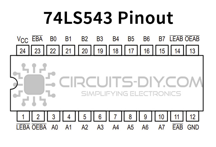
| Pin No. | Pin Name | Description |
|---|---|---|
| 1 | LEBA’ | Active Low B to A Latch Enable Input |
| 2 | OEBA’ | Active Low B to A Output Enable input |
| 3 | A0 | Data Input 0, Port A |
| 4 | A1 | Data Input 1, Port A |
| 5 | A2 | Data Input 2, Port A |
| 6 | A3 | Data Input 3, Port A |
| 7 | A4 | Data Input 4, Port A |
| 8 | A5 | Data Input 5, Port A |
| 9 | A6 | Data Input 6, Port A |
| 10 | A7 | Data Input 7, Port A |
| 11 | EAB’ | Active Low A to B Enable Input |
| 12 | GND | Ground Pin |
| 13 | OEAB’ | Active Low A to B Output Enable input |
| 14 | LEAB’ | Active Low B to A Latch Enable Input |
| 15 | B7 | Data Input 7, Port B |
| 16 | B6 | Data Input 6, Port B |
| 17 | B5 | Data Input 5, Port B |
| 18 | B4 | Data Input 4, Port B |
| 19 | B3 | Data Input 3, Port B |
| 20 | B2 | Data Input 2, Port B |
| 21 | B1 | Data Input 1, Port B |
| 22 | B0 | Data Input 0, Port B |
| 23 | EBA’ | Active Low B to A Enable Input |
| 24 | Vcc | Chip Supply Voltage |
Applications
The 74F543 IC has a wide array of applications. A few of them are mentioned down below:
- Usually used in applications such as building automation & GUI interface circuitry.
74F543 Datasheet
You can download the datasheet for 74F543 Octal Registered Transceiver IC from the link given below:
See Also: 74LS138 1-To-8 Decoder/Demultiplexer IC – Datasheet | 74LS45 BCD to Decimal Decoders/Drivers IC – Datasheet | 74LS31 Hex Delay Element/Delay Line Generator IC – Datasheet