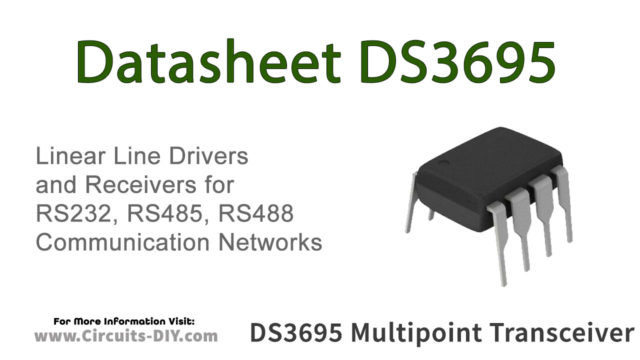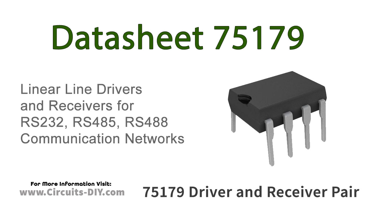
The SN75179 is a differential driver and receiver pair designed for balanced transmission-line applications. It is designed to improve the performance of full-duplex data communications over long bus lines. The SN75179B driver output provides limiting for both positive and negative currents. The receiver features high input impedance, input hysteresis for increased noise immunity, and input sensitivity of ±200 mV over a common-mode input voltage range of –7 V to 12 V.
The driver provides thermal shutdown for protection from line fault conditions. Thermal shutdown is designed to occur at a junction temperature of approximately 150°C. The SN75179B is designed to drive current loads of up to 60 mA maximum.
75179 Pinout
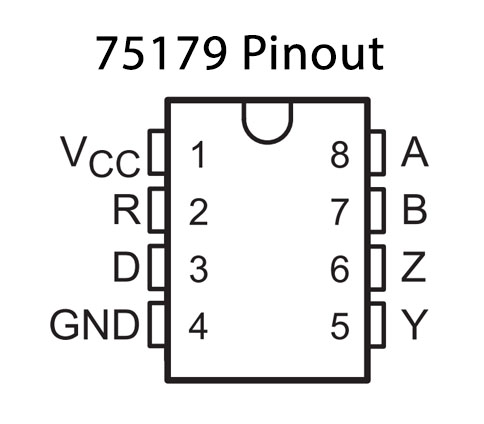
75179 Pin Configuration
| Pin No | Pin Name | Description |
|---|---|---|
| 1 | VCC | Collector Supply Voltage |
| 2 | R | Receiver Pin |
| 3 | D | Driver Pin |
| 4 | GND | Ground |
| 5 | Y | Input Pin Y2 |
| 6 | Z | Input Pin Z2 |
| 7 | B | Input Pin B1 |
| 8 | A | Input Pin A1 |
75179 Key Features
- Bus Voltage Range –7 V to 12 V
- Positive- and Negative-Current Limiting
- Driver Output Capability 60 mA Max
- Driver Thermal-Shutdown Protection
- Receiver Input Impedance 12 kΩ Min
- Receiver Input Sensitivity ±200 mV
- Receiver Input Hysteresis 50 mV Typ
- Operates From Single 5-V Supply
- Low Power Requirements
Application
- Balanced transmission-line applications
You can download this datasheet for 75179 Differential Driver and Receiver Pair from the link given below: