The 74LS379 IC is a 4-bit D-Type parallel register with a buffered common enable. 74LS379 IC consists of four edge-triggered D-type flip-flops with individual D inputs and Q and Q’ outputs. The Clock (CP) and Enable (E) inputs are common to all flip-flops. When E is HIGH, the register will retain the present data independent of the CP input. The IC is designed to prevent false clocking by transitions on the E (Enable) input. 74LS379 IC has a wide range of working voltage, a wide range of working conditions, and directly interfaces with CMOS, NMOS, and TTL. The IC 74LS379 is smaller in size and it has a much faster speed which makes it reliable in every kind of device.

What is a D-Type Flip-Flop?
A D-type flip-flop is a clocked latch with bi-stable states that operates with a delay in input by one clock cycle. Thus, by cascading many D-type flip-flops delay circuits can be created, which are used in many applications such as in digital television systems. A D-type flip-flop is also known as a D flip-flop or a delay flip-flop.
74LS379 Key Features & Specifications
- Function: D-Type latch
- Channels (#): 4
- Technology Family: LS
- VCC (Min): 4.75V
- VCC (Max): 5.25V
- Input type: Bipolar
- Output type: Push-Pull
- Clock frequency (Max): 35Mbps
- IOL (Max): 8mA
- IOH (Max): -0.4mA
- Propagation speed: (TPD 5-10ns)
- 8-Bit High Speed Parallel Registers
- Positive Edge-Triggered D-Type Flip Flops
- Fully Buffered Common Clock and Enable Inputs
- True and Complement Outputs
- Input Clamp Diodes Limit High Speed Termination Effects
74LS379 Pinout
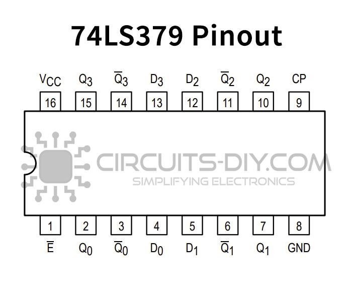
| Pin No. | Pin Name | Description |
|---|---|---|
| 1 | E’ | Active Low Enable Pin |
| 2 | Q0 | Register Output Pin Q0 |
| 3 | Q0′ | Complementary Register Output Pin Q0 |
| 4 | D0 | Data Input Pin D0 |
| 5 | D1 | Data Input Pin D1 |
| 6 | Q1′ | Complementary Register Output Q1 |
| 7 | Q1 | Register Output Pin Q1 |
| 8 | GND | Ground Pin |
| 9 | CP | Clock Pulse Input |
| 10 | Q2 | Register Output Pin Q2 |
| 11 | Q2′ | Complementary Register Output Q2 |
| 12 | D2 | Data Input Pin D2 |
| 13 | D3 | Data Input Pin D3 |
| 14 | Q3′ | Complementary Register Output Q3 |
| 15 | Q3 | Register Output Pin Q3 |
| 16 | Vcc | Chip Supply Voltage |
Applications
The 74LS379 IC jas a wide array of application, a few of them are as follows:
- They are usually used in applications such as, in communication lines where demultiplexing of a data line into several parallel lines is required.
- They are also used to convert serial input data into a parallel output format.
74LS379 Datasheet
You can download the datasheet for 74LS379 Quad 4-Bit D-type Parallel Register IC from the link givrn below:
See Also: 74LS56 50-to-1 Frequency Divider IC – Datasheet | 74LS73 Dual JK Negative Edge Triggered Flip-Flop IC – Datasheet | 74LS46 BCD – 7 Segment Decoder IC – Datasheet