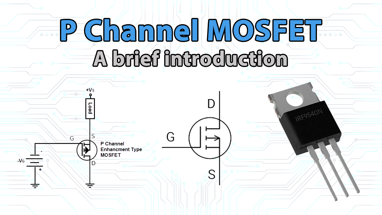
Overview of P Channel MOSFET
Two charge carriers—electrons and holes—are responsible for determining the conduction level in a bipolar junction transistor (BJT). The JFET, on the other hand, is a unipolar device since its conduction is solely dependent on either electron (n-channel) or holes (p-channel). P channel MOSFETs are a subtype of MOSFET in which the bulk of the charge carriers is holes in the channel. The bulk of charge carriers, such as holes, will travel along the channel after this MOSFET is turned on. This MOSFET differs from N channel MOSFET in that the bulk of charge carriers in an N MOSFET are electrons. Below are symbols for P Channel MOSFETs in enhancement mode and depletion mode. Want to look at more different types of transistors, you can look at this Electronic Part to see more products, datasheets, and specifications about the transistors.
The body of the P- channel MOSFET is composed of an n-region, and the P- Channel region is situated between the two terminals, source, and drain. This kind of MOSFET has three terminals, similar to the N channel MOSFET’s source, drain, and gate. The substrate employed in this MOSFET is n-type, and both the source and drain terminals are extensively doped with p-type materials.
Driving the High-Side (HS) Switch gate
This picture shows one example of the gate driving circuit for HS P-channel power MOSFET.

The standard gate driving circuit for an N-channel power MOSFET was enhanced in the circuit by the addition of Dz, Rz, and Ch. The input capacitance of the P-channel MOSFET must be significantly bigger than the capacitor “Ch,” which stores DC voltage between the higher and lower gate drive circuits. Dz maintains the gate to source voltage between -Zener voltage and zero.
P -channel Enhancement MOSFET
P channel improvement The n-substrate of a MOSFET is simply built with minimal doping. Here, two strongly doped p-type materials are separated by an L-shaped channel. The substrate, which is typically referred to as the dielectric layer, is coated with a thin layer of silicon dioxide. The source (S) and drain (D) of this MOSFET are made of two P-type materials, and the gate (G) terminal is made of aluminum by plating on the dielectric. Here, the GND serves as the sole connection between the source and body of the MOSFET.

The +ve concentration of the charges will settle under the dielectric layer when a negative voltage is applied to the gate (G) terminal due to the capacitance effect. The repulsive forces will drive the electrons that are present at the n substrate to migrate. When a negative voltage is given to the drain terminal, the voltage differential between the gate and drain also lowers. This causes the conductive channel width to narrow toward the drain region, allowing current to flow from the source to the drain.
The MOSFET’s created channel acts as a barrier to the flow of current from source to drain. Here, the channel’s resistance is mostly influenced by its side view, and its cross-section is again influenced by the negative voltage applied at the gate terminal. As a result, a MOSFET is referred to as a voltage-controlled device because it allows the voltage applied at the gate terminal to regulate the current flow from the source to the drain. It is referred to as a P-Channel Enhancement MOSFET when the channel is formed by the concentration of holes and the channel’s current flow is improved as a result of a rise in the negative gate voltage.
How Are P Channel MOSFETs Tested?
- The multimeter must first be tuned to the diode range.
- Place the MOSFET with its printed side facing you on any wooden table.
- Shorting the MOSFET’s drain and gate terminals with the probe of a digital multimeter will first allow the device’s internal capacitance to discharge, making it essential for the MOSFET testing process.
- Now connect the black probe of the multimeter to the drain terminal and the red probe to the source terminal.
- An open circuit reading will appear on the multimeter display.
P channel Depletion MOSFET
In order to create an n-channel depletion MOSFET, the p-channel depletion MOSFET design is inverted. Because there are p-type impurities present, the channel in this MOSFET is pre-built. The minority charge carriers, such as n-type electrons, are drawn to the p-type channel after a negative (-) voltage is supplied at the gate terminal. When a drain is reverse-biased in this situation, the device starts to conduct, but when the negative voltage inside the drain is increased, a depletion layer forms.

This region is primarily reliant on the layer concentration that the holes create. The conductivity value of the channel will be impacted by the region width of the depletion layer. Therefore, the region’s voltage values can be varied to control the current flow. Finally, the source will remain at 0 while the gate and drain remain in the negative polarity.
How is A P-Channel MOSFET Used?
The motor control MOSFET switch complementary circuit is depicted below. The P channel and N channel of two MOSFETs are used in this switch circuit to operate the motor in both directions. In this circuit, the motor is simply linked between the common drain and the GND reference to create a bi-directional switch using a dual supply.

P-channel MOSFETs linked to the circuit will switch ON once the input voltage is LOW and N-channel MOSFETs will turn off because their gate-to-source junctions are biased negatively, which causes the motor in the circuit to rotate in one direction. The +VDD supply rail is used to control the motor in this instance. Similar to how the P-channel device turns OFF when the input is HIGH, the N-channel MOSFET switches ON because its gate-to-source junction is biased positively. Due to the motor’s terminal voltage being supplied through the -VDD supply rail, the motor now rotates in the opposite direction.
Then the +ve supply is switched to the motor for the forward direction using a P-channel type MOSFET, and the -ve supply is switched to the motor for the reverse direction using an N-channel type MOSFET.
Advantages of P-Channel MOSFET
- Due to the simplicity of this MOSFET design, it can be used in applications with limited space, such as non-isolated POLs and low-voltage drives.
- This is the high-side switch place’s streamlined gate-driving strategy, which frequently lowers total cost.
- When MOSFETs are used at low voltages, their efficiency is greater.
- MOSFETs have a higher input impedance than JFETs do.
- Due to low channel resistance, they have good drain resistance.
- Making them is really straightforward.
- Compared to JFETs, it offers high-speed operation.
Disadvantages of P-Channel MOSFET
- The MOSFET’s thin oxide layer will make it vulnerable to damage when induced by electrostatic charges.
- These are not stable when high voltages are used.
Related posts:
 Top 5 Omron Relays For Home Automation And Their Prospects
 Different Types of Resistors and Their Applications Explained
 Where can I buy Electronic Components for DIY use at one time?
 Microprocessors vs Microcontrollers: Unveiling the Differences
 Nuvoton NuMaker – Volcano – Getting Started – LED Blink
 The Power of Electronic Components: A Comprehensive Guide


