CD40109 belongs to the CD4000 IC series. CD40109 contains four low-to-high voltage level shifting circuits. Each circuit will shift a low voltage digital logic input signal (A, B, C, D) with logical 1 = VCC and logical 0 = VSS to a higher voltage output signal (E, F, G, H) with logical 1 = VDD and logical 0 = VSS. When operated in the mode VCC > VDD, the CD40109 will operate as a high-to-low level shifter. The CD40109BMS also features individual three-state output capability. A low level on any of the separately enabled three-state output controls produces a high impedance state in the corresponding output. The output of the IC always comes in TTL which makes it easy to work with other TTL devices and microcontrollers. CD40109 is smaller in size and it has a much faster speed which makes it reliable in every kind of device.
Voltage Level Shifter
Voltage Level Shifter serves as an interface between different supply and input/output voltage levels. Voltage level shifters cover a range from single-bit to 32-bit widths. They also act as an interface between applications with different supply voltage and I/O voltage levels.
CD40109 Key Features
- High Voltage Type (20V Rating)
- Independence of Power Supply Sequence Considerations
- VCC can Exceed VDD
- Input Signals can Exceed Both VCC and VDD
- Up and Down Level Shifting Capability
- Three-State Outputs with Separate Enable Controls
- 100% Tested for Quiescent Current at 20V
- 5V, 10V and 15V Parametric Ratings
- Maximum Input Current of 1µA at 18V Over Full Package Temperature Range; 100nA at 18V and +25oC
- Noise Margin (Over Full Package/Temperature Range)
- 1V at VCC = 5V, VDD = 10V
- 2V at VCC = 10V, VDD = 15V
- Standardized Symmetrical Output Characteristics
CD40109 Pinout
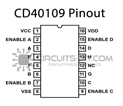
| Pin No | Pin Name | Description |
|---|---|---|
| 1 | VCC | Collector Supply Voltage |
| 2 | ENB-A | Enable Pin A |
| 3 | A | Input Pin A |
| 4 | E | Output Pin E |
| 5 | F | Output Pin F |
| 6 | B | Input Pin B |
| 7 | ENB-B | Enable Pin B |
| 8 | VSS | Source Supply |
| 9 | ENB-C | Enable Pin C |
| 10 | C | Input Pin C |
| 11 | G | Output Pin G |
| 12 | NC | No Connection |
| 13 | H | Output Pin H |
| 14 | D | Input Pin D |
| 15 | ENB-D | Enable Pin D |
| 16 | VDD | Drain Supply |
Application
- High or Low Level Shifting with Three-State Outputs
- for Unidirectional or Bidirectional Bussing
- Isolation of Logic Subsystems Using Separate Power
- Supplies from Supply Sequencing, Supply Loss and
- Supply Regulation Considerations
CD40109 Datasheet
You can download the datasheet for CD40109 Low to High Voltage Level Shifter form the link given below:
See Also: 74LS27 Triple 3-Input NOR Logic Gate IC – Datasheet | 74LS04 Hex Inverter IC / NOT Gate IC – Datasheet | 74LS13 Dual 4 – Input Schmitt Trigger/ Hex Inverter IC – Datasheet
Related posts:
 29F040 512k 90ns CMOS Flash Memory - Datasheet
 LM3403 Quad Operational Amplifier - Datasheet
 CD4077 Quad EXCLUSIVE-NOR Gate - Datasheet
 74LS574 Octal Edge Triggered D-Type Flip-Flop IC With Tri-State Outputs
 2SC644 NPN General Purpose Amplifier - Datasheet
 2N6059 NPN Power Darlington Transistor - Datasheet


