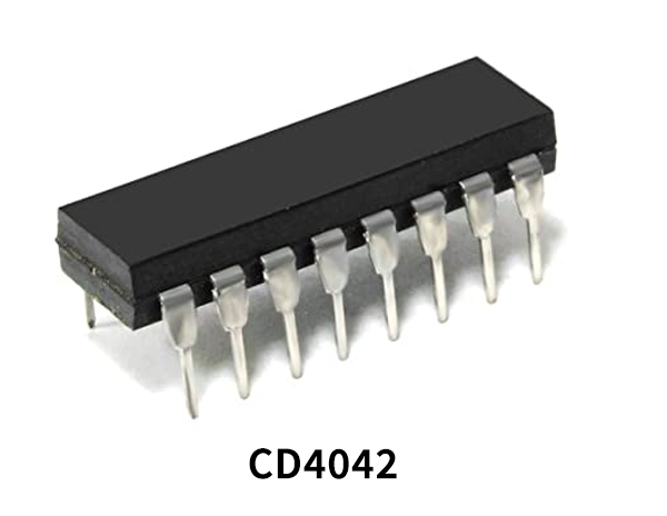
CD4042 consists of four clocked ‘‘D’’ latches, designed by using monolithic complementary MOS (CMOS) technology, integrated with P- and N-channel enhancement mode transistors. For polarity e 0; the information present at the data input is transferred to Q and Q during 0 clock level; and for polarity e 1, the transfer occurs during the 1 clock level. When a clock transition occurs (positive for polarity e 0 and negative for polarity e 1), the information present at the input during the clock transition is retained at the outputs until an opposite clock transition occurs. The output of the IC always comes in a 16 – pin hermetically sealed dual in line package (DIP). The IC offers many features such as high noise immunity, low thermal dissipation, and ESD barring, etc.
What is a D-Type Latch?
A D-type Latch is a clocked latch which has two stable states. A D-type latch operates with a delay in input by one clock cycle. Thus, by cascading many D-type flip-flops delay circuits can be created, which are used in many applications such as in digital television systems. A D-type latch is also known as a D flip-flop or a delay flip-flop.
CD4042 Key Features
- Wide supply voltage range 3.0V to 15V
- High noise immunity 0.45 VDD (typ.)
- Low power TTL compatibility Fan out of 2 driving 74L or 1 driving 74LS
- Clock polarity control
- Fully buffered data inputs
- Q and Q outputs
CD4042 Pinout
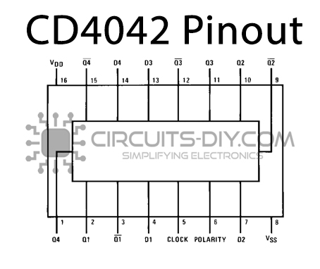
| Pin No | Pin Name | Description |
|---|---|---|
| 1 | Q4 | Output of Data Pin D4 |
| 2 | Q1 | Output of Data Pin D1 |
| 3 | Q1′ | Inverting Output of Data Pin D4 |
| 4 | D1 | Data input of flip flop 1 |
| 5 | CLK | Clock input of the IC |
| 6 | POLARITY | Used to change the Rising time of the output |
| 7 | D2 | Data input of flip flop 2 |
| 8 | VSS | source supply |
| 9 | Q2′ | Inverting Output of Data Pin D2 |
| 10 | Q2 | Output of Data Pin Data Pin D2 |
| 11 | Q3 | Output of Data Pin Data Pin D3 |
| 12 | Q3′ | Inverting Output of Data Pin D3 |
| 13 | D3 | Data Input of flip flop 3 |
| 14 | D4 | Data Input of flip flop 4 |
| 15 | Q4′ | Inverting Output of Data Pin D4 |
| 16 | VDD | Drain supply |
Application
- Bounce elimination switch
- Buffer Storage
- Data transfer
- Holding Register
- General Digital Logic
CD4042 Datasheet
You can download the datasheet for CD4042 Quad Clocked D Latch from the link given below:
See Also: CD4516 Binary Up Down Counter – Datasheet | CD4067 16-channel Analog Multiplexer/Demultiplexer Datasheet | CD4011 Quad 2-input NAND Gate – Datasheet