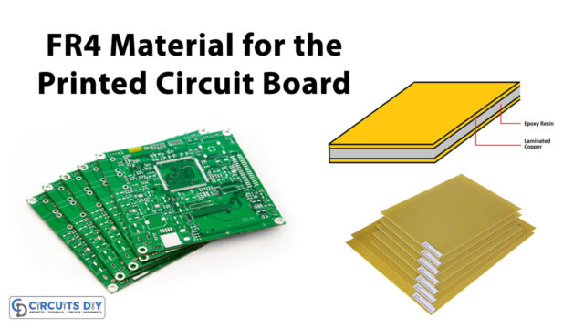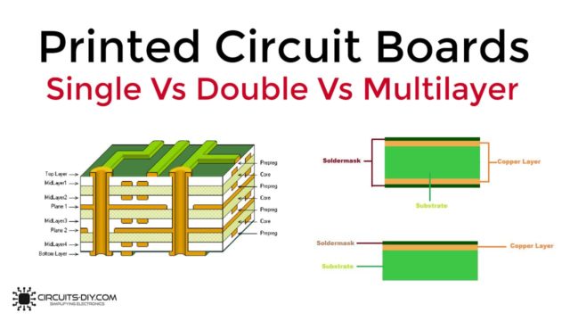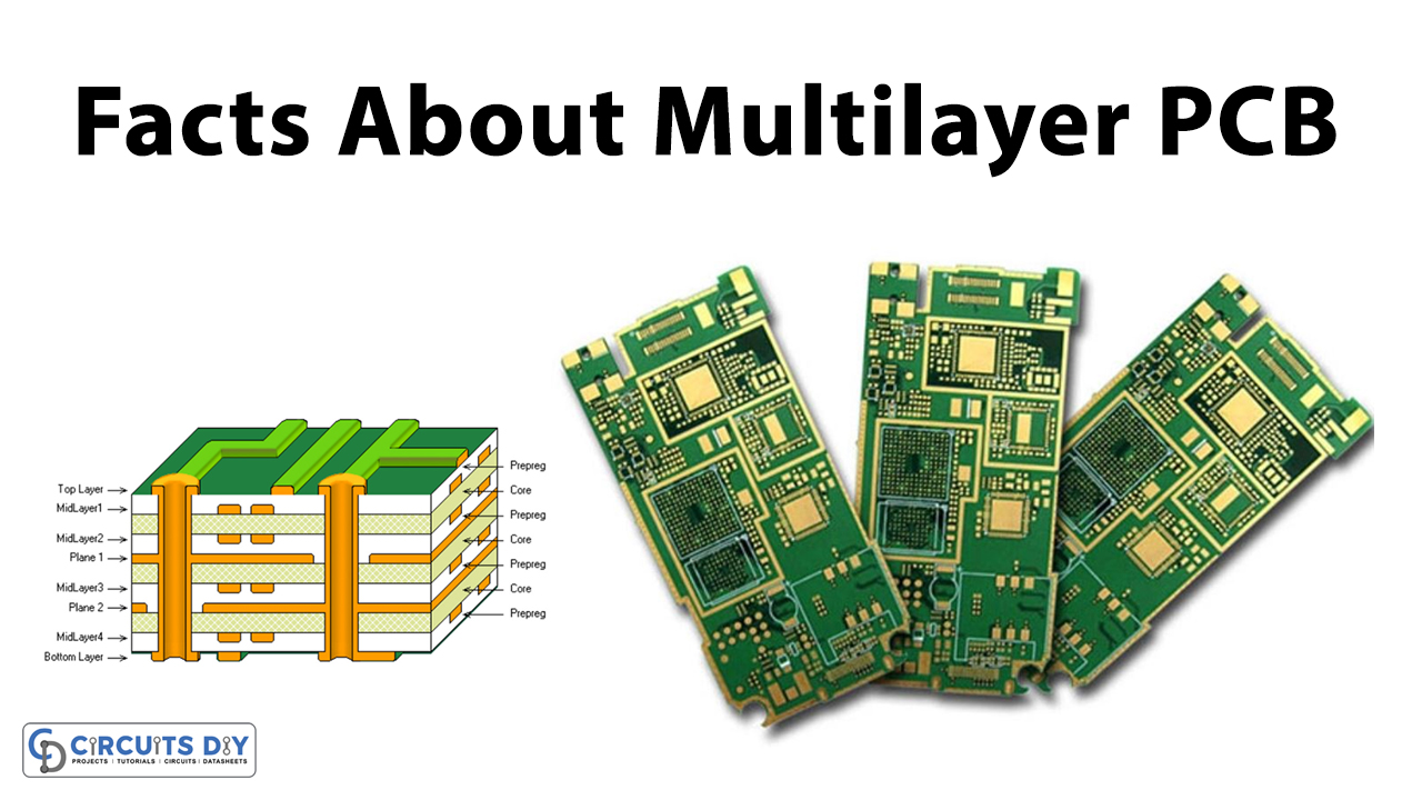
Multilayer PCB
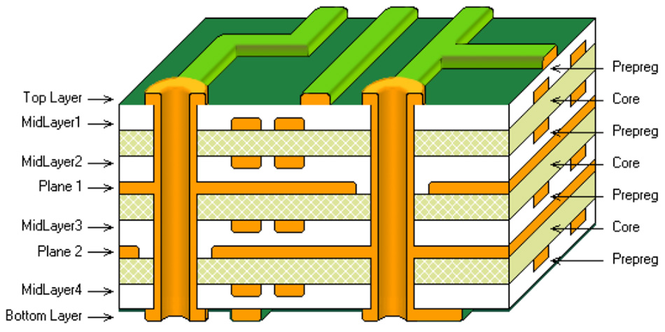
Multi-layer PCBs contain three dual-size copper layers allowing a complete layer for the ground plane. It can support thousand of components and ten thousand vias. Most of the multi-layers have less than 10 conducting layers and have a thickness of 1.5mm. Here are some facts about multilayer PCB
Some Beneficial Facts of Multilayer
The single-layer PCB has just one base layer. In the same vein, the double layer has a double layer of the substrate. However, the multilayer contains multiple substrates layers. Some of the beneficial facts of this PCB are:
- Mainly, It is more useful for difficult and sophisticated circuits and complex devices. Therefore, if a device needs many circuits, it can easily be designed on a multi-layered PCB
- Secondly, they have great quality because they require more planning in the process of making a multi-layer circuit board. Many of the designs on this type of PCB includes an impressive impedance feature.
- Further, they are more effective and less problematic and have a remarkable operating capacity. They can effortlessly run at a higher speed which is vital in advanced devices for better performance
- Then, they are tinier in size and lighter in weight
- Also, they are designed to work with a single connection which simplified circuits and electronic devices. This also decreases the weight of the circuit
- In short, Multi-layer PCB boards can easily tolerate difficult conditions. It has a high durability rate
Facts About Manufacturing Process
- Multilayer uses almost seven layers in manufacturing. It includes the first layer of copper foil. Then the layer of prepreg. Again, a layer of copper foil. Further, a PCB core layer. Then a layer of copper foil. Again, the prepreg. And finally, again the copper foil layer.
- To melt the prepreg, high pressure and temperature are applied. This joins all the layers effectively
Application Facts About Multilayer PCB
There are so many applications of the multilayer PCB. Yet the reason or the faces that why they are used in those applications are described below:
- Since it reduces the size and can easily use in small devices. Hence, used in Smartphones
- Multilayer PCBs have better heat transfer ability than other PCBs. Hence used in X-ray machines which
- In computers, the circuits are difficult and complicated. Therefore multilayer PCBs are used
- Heart monitoring devices measure the heartbeat, etc, so it needs to be ideal. Thus, uses a multi-layer
- Having more layers inside the board enables complex circuitry. Therefore it is used in the satellite applications
- Military equipment and devices need excellent quality with outstanding integrity. Therefore it can utilize in defense and military applications
- It has a relatively higher speed since components are close to each other. Hence, Exist Fibre optics
- They have a higher operating capacity and can run at higher speeds. That’s why used in GPS technology
- More layer means that the board is thicker. Is more durable. That’s maybe the reason that it is used In nuclear detection system
- Due to its versatility of higher speed, outstanding integrity, high durability rate, enormous stability, better heat transfer, immense operating capacity, it can be used in weather analysis