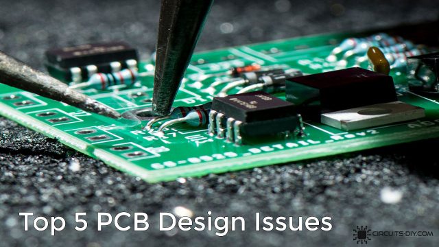
A PCB board works together to form a complete system to power our devices. As we get further into the PCB design process, first let me get you familiar with a couple of commonly used words from the PCB glossary.
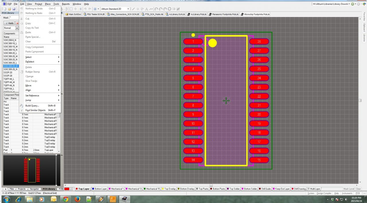
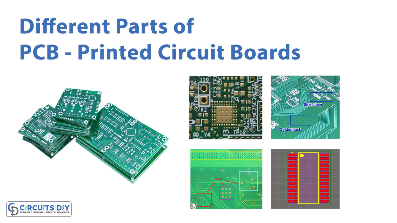
Pad
A pad is a small surface of copper in a PCB where the components are mounted and soldered. It provides mechanical support to the components. Normally there are 2 types of pads; surface-mount pad and thru-hole pad. In thru-hole pads, pins of the components are introduced so they can be soldered from the opposite side from which the component was inserted. A surface mount pad is a rectangular or square copper area used for mounting surface-mount components.

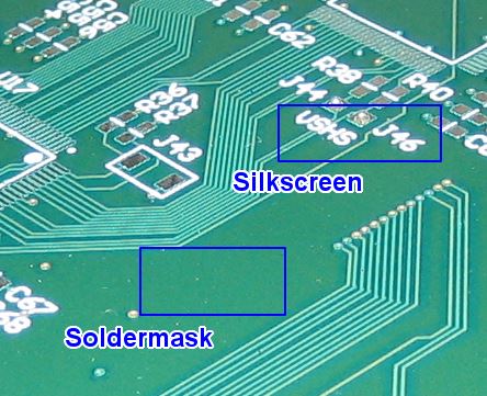
Soldermask
Soldermask also called solder resist is a thin layer covering copper traces on both the top side and bottom side to help ensure PCB reliability and high performance. It shields the entire PCB from a possible short circuit. Resin is usually selected as the leading material of the solder mask because it works excellent in terms of humidity and high-temperature resistance.
Silkscreen
The Silkscreen is the topmost layer of a Printed Circuit Board (PCB). It is used as a reference indicator for placing components on a PCB Board. The silkscreen is used to specify useful information on the PCB that can help/assist users during assembly. It is used to mark component values, part numbers, polarity, etc. It requires a specifically formulated ink whose standard color is white, but it can also be red, black, yellow, and blue.
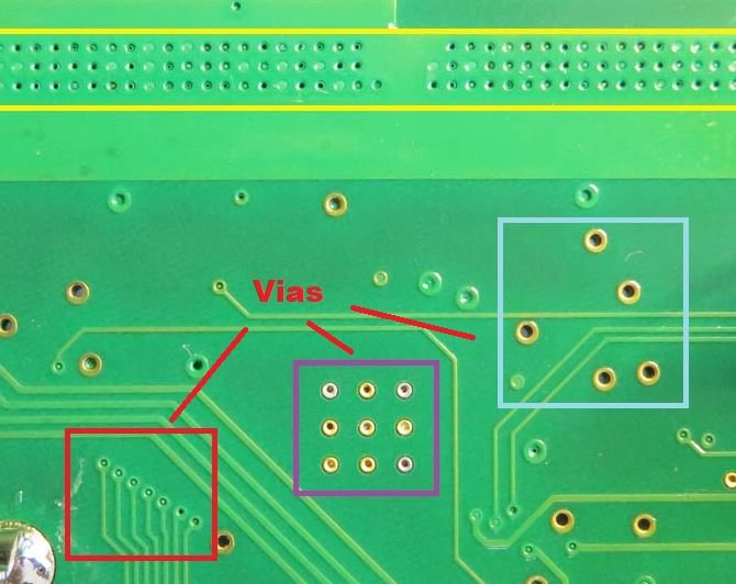
Via
Vias are used to electrically join traces and pads on different layers of a PCB. Connecting multiple layers of the board makes it possible to reduce the size of the PCB. A via is constructed by placing copper pads on each layer of the PCB and drilling a hole through them. The hole can be made conductive through electroplating or by placing copper cylinders directly in the drilled holes.
There are three main types of Vias used in a Printed Circuit Board:
Through-Hole Via: This Via goes right through the PCB board from top to bottom and is used to connect all the layers of a PCB.
Blind Via: This Via connects the outermost layer of a PCB to the next layer. It is called blind via because it can not be seen on the other side of the board.
Buried Via: This Via cannot be seen on the surface of the board. and is used to connect internal layers of a PCB.
Footprint
Footprint or land pattern is used during board layout and is where an electronic component gets soldered onto the PCB. It consists of several layers of information, including the copper lands, silkscreen, solder mask, and solder paste. A footprint’s characteristics vary depending on the mechanical dimensions and tolerances of the component.