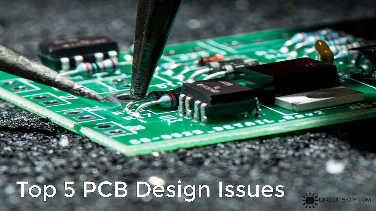
PCB Designing process is basically a string of industrial design steps, essential for efficient mass production of PCBs while ensuring the quality of design & minimizing the risk of troubleshooting. PCBs or printed circuit boards serve as the backbone of any design industry. Whether it be small-scale consumer electronics production or a large scale operation pertaining to the design and development of industrial electronic components, PCBs have found their way into almost every aspect of design technology. PCB designing is an intricate & complex process in which even the most common mistakes can occur. So, In today’s article, we are going to go over the Top 5 PCB Design Issues Faced In PCB Manufacturing & their possible solutions.
JLCPCB is the foremost PCB prototype & manufacturing company in china, providing us with the best service we have ever experienced regarding (Quality, Price Service & Time).
Top 5 PCB Design Issues Faced In PCB Manufacturing
1) Incorrect Layout of Switching Regulators
Linear voltage regulators may be cheaper than conventional switching regulators, but they are not as efficient as switching regulators. Generally, most design engineers tend to select linear voltage regulators due to their ease of use and efficiency. But one should keep in mind that while being efficient in use, linear voltage regulators consume a tremendous amount of power, leading to extensive heat dissipation. On the other hand, Switching regulators are more complex, but much more efficient. However, they require more careful layouting on the PCB, so the datasheet guidelines must be followed closely.

2) Design & Drawing Mismatch
Comparative discrepancies in Design & Drawing can cause major faults in the final design phase of a PCB. So, make sure to double-check for things such as drawing to data dimensions, hole quantity, pad size, and revision levels. The take-away from this is to always double-check your designs with respect to the initial schematic.
3) Acid Traps
Acid traps occur when two traces join at a highly acute angle resulting in a possibility that the etching solution that removes copper from the blank board will get stuck/trap at these junctions. This cause traces to become disconnected from their assigned nets and leave these traces open circuited. The issue of Acid traps has been reduced in recent years by fabricators switching to the use of photo activated etching solutions.
4) Tombstoning of Components
If small passive SMT electronic parts are solder to a PCB assembly using a reflow process, There lies a tendency for them to lift up on one end and “tomb stone”. Usually, the source of tombstoning can be incorrect landing patterns and imbalance thermal relief to the pads of the device. Tombstoning can be effectively mitigated by the use of proper DFM checks.

5) Not Enough Width of High Power Traces
The minimum PCB trace width threshold won’t be sufficient if the PCB Board traces has to house currents greater than 500mA. A trace on an outer layer can carry more than an internal trace for the same thickness. This is because the external trace has superior airflow and thermal dissipation. The width depends on how much copper is being used for that layer. Most PCB manufacturers allow you to choose from various copper weights from 0.5 oz/sq.ft to 2.5 oz/sq.ft.

Related posts:
 What is Flex PCB? Advantages Disadvantages & Applications
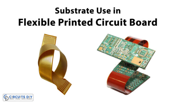 Substrate Use in Flexible Printed Circuit Board
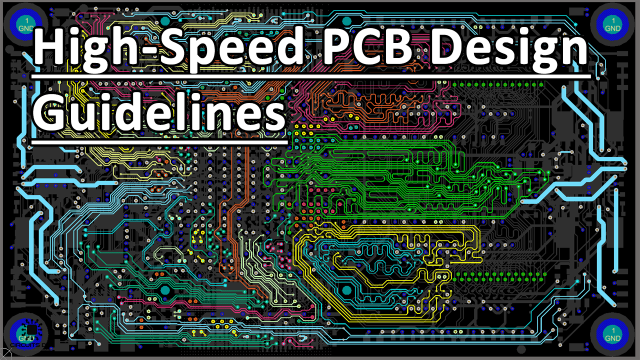 High-Speed PCB Design Guidelines
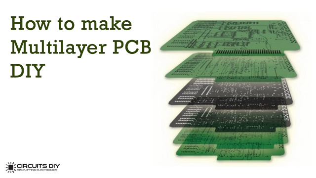 How To Make A Multilayer PCB At Home - A Beginners Guide
 SMT PCB Assembly Process - A Complete Guide For Beginners
 Build Your Private Online Parts Warehouse in JLCPCB