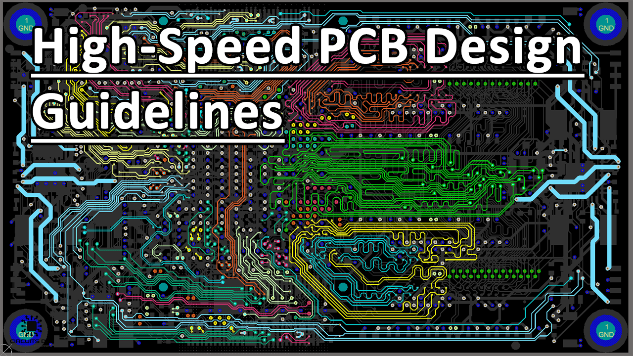
In today’s world of high-frequency signals and fast switching devices, it is highly likely that you will be asked to do a high-speed PCB design. When a person thinks about the term “high speed”, they are likely to default to clock rate. However, a high-speed design has nothing to do with clock rates. It has everything to do with the rate at which the signal level swings between digital states. The term “high speed” refers to the amount of time a digital signal takes to switch between OFF and ON states. Examples of high-speed signals include clock signals and high-speed communication ports.
PCB boards that are classified as “good” for high-speed signals are typically designed to accommodate frequencies from 500MHz to 2GHz. This is because, in this frequency range, signal integrity issues influence PCB performance, and board materials have an impact on overall board design. Poor layouts can result in performance issues when fabricated PCBs are put into testing or production use.
What is high speed PCB design?
High-speed PCB design is any design where the quality of your signals starts to get affected by the physical characteristics of your circuit board, like your layout, layer stack-up, interconnections, etc. High-speed PCB design is different due to the attention paid to these issues. Efficient fabrication of printed circuit boards (PCBs) utilized in high-speed circuitry is critical to the end result. However, here are some more requirements and design practices associated with high-speed circuits that you will need to become familiar with. We’ll describe some of those to get you started in understanding high-speed design guidelines.
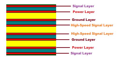
1) Board Stackup
Board stack up is one of the most important parts of PCB design. The order of stack up is very important in ensuring that the design comes out as expected for a number of technical reasons. High-speed signals require a reference plane on an adjacent layer in order to decrease the loop inductance for that signal. Another consideration is if you can create the stack up such that the power planes are very close to each other, you can reduce the need for small value decoupling capacitors in your design.
2) Component Placement
There are some crucial components that must be well-defined for board functionality, such as critical power locations and input/output points. High-speed circuitry will often require very close placement of some components to minimize the distance that signals need to travel. Additionally, components need to be placed so that signal traces do not cross split planes and each signal has a clear return path. You may also encounter larger than normal thermal issues in your designs. This means high-speed designs may require more cooling and you need to consider airflow of the circuit.
3) Routing High-Speed PCB Circuitry
With high speeds reaching well into the sub-nanosecond regime, and to support high-speed networking equipment. Every designer should keep some basic high-speed PCB routing guidelines in mind. Some of them are given below:
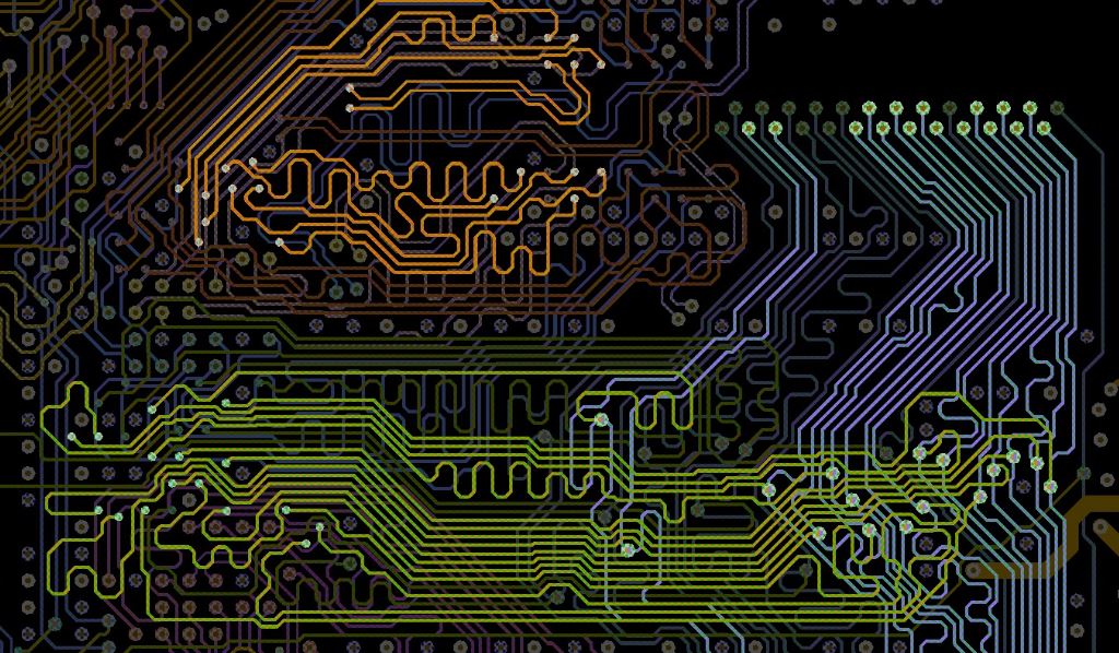
- Minimize the use of vias: Vias change the characteristic impedance of the trace and can cause reflection of signals. If you want to use vias with differential signal traces, place them in both the traces to ensure that their effect is equal in both traces.
- Prefer shorter trace lengths: Signals lose energy over time because of dielectric absorption. This means you should opt to use shorter traces in order to minimize attenuation.
- Length Matching: Matching the lengths of two coupled traces will ensure that your traces arrive at the same time and in sync with your clock rates.
- Trace Spacing: The closer your traces are to each other, the more susceptible they become to noise and other forms of signal interference. By not placing your traces close to each other, you’ll reduce the amount of noise on your board.
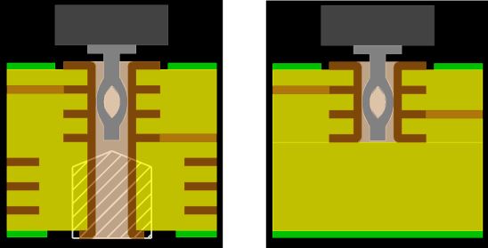
- Back Drilling of Vias: Length of vias should be minimized on traces as they can create an impedance discontinuity. Any vias present on an interconnect should be back drilled. As any remaining via stub represents another impedance discontinuity, thus they present another opportunity for signal reflection.
- Rounding Trace Corners: By rounding trace corner we can reduce the level of EMI radiated by a signal. This is because the abrupt changes in the traces lead to higher levels of capacitance and also cause signal reflections.