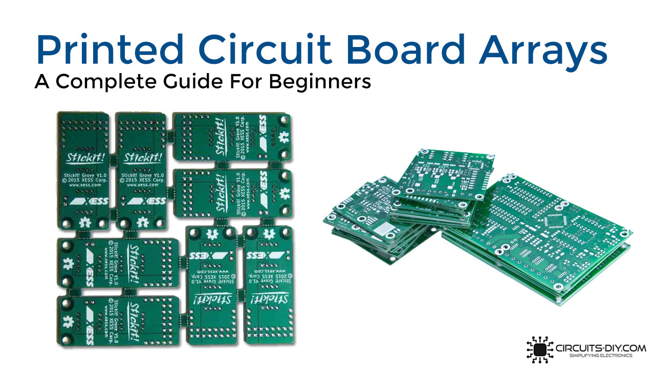
The term array is used interchangeably in the PCB design industry. Essentially, it means a block containing a grid of similar elements. PCB Fab houses generally use printed circuit board arrays in order to mass produce multiple copies of the same circuit board. This allows manufacturers to cut down on production costs while maintaining design quality. Also, it is much easier to load and store PCB arrays into pick and place machines in contrast with loading each separate board one at a time. So, In today’s guide, we are going to take a deep look into printed circuit board arrays and their construction.
What are PCB Arrays?
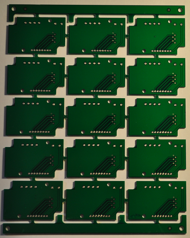
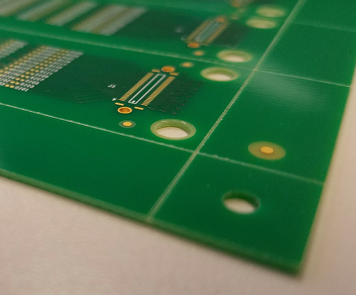
Printed Circuit board arrays are basically combining a single PCB multiple times to make a larger array of connected boards. This process is referred to as “stepping out” the individual boards. It is often referred to as “step and repeat.” PCB Arrays are very useful when it comes to PCB assembly. You can easily program an assembly machine to simply step and repeat the PCB array grids of the same types & number of components to quickly finish a larger set of boards.
Common Parts of A Printed Circuit Board Array
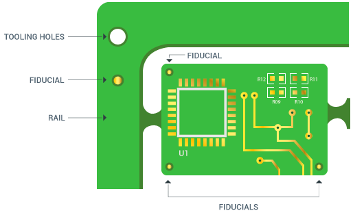
1) Rails
Rails allow easy handling of PCB arrays. It is just extra insulative material on the four sides of the PCB array that promotes easy loading and storage of PCB arrays. You can install rails either on all four sides of the PCB array or only two sides. You can reduce per board price by using rails on only two sides.
2) Fiducials
A fiducial mark is basically a copper pad with the exact same surface finish as that of the rest of the board. Fiducial markers provide support to automated assembly equipment by adjusting their alignment targets. Typically, three fiducials are needed on an array and they usually go on the rails. The ideal size for fiducial markers is .050”.
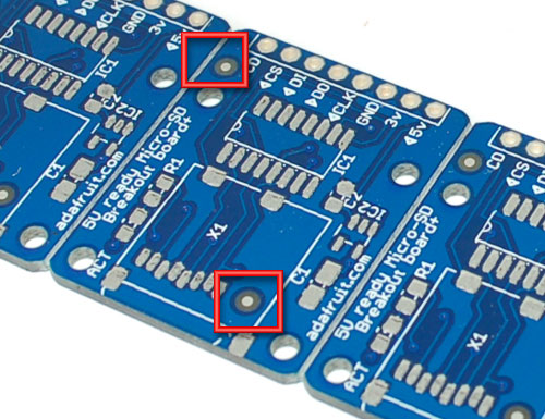
3) Tooling Holes
Tooling holes basically hold down the PCB array during the assembly process. These holes are drilled on the four corners of the PCB array or somewhere on the rail itself. They also aid in array alignment and orientation when assembling the board. The typical size is .125”(non-plated).
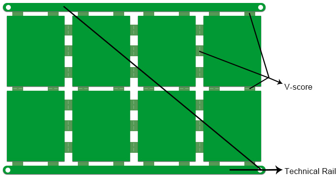
4) Scoring
Scoring is basically cutting a small “V” groove along the length of the board where they will be separated. The groove is generally 1/3rd from the top, 1/3rd from the bottom, leaving 1/3rd of the material remaining in place to hold the boards together. When scoring your PCB array, one should also be careful that no parts should be placed within .250” of the edge of the board. If they are closer than that, there is the possibility that the parts could come loose during the de-paneling process. If the board thickness is more than .062” and the score line is long, it can result in excessive force being applied to the boards in order to separate them. This can cause accidental breakage of the PCB array grids.
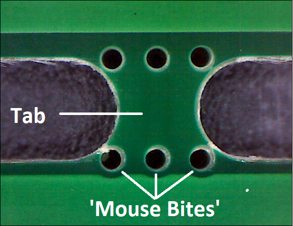
5) Tab Rout
Tab Rout is basically a small perforated tab on the board that is provided to remove a single grid from the PCB array. They are pretty sturdy so as to deal with the mechanical stress of the entire fabrication process but less sturdy than the scored rails. Thus they can be easily separated without hurting the PCB array. A big advantage to tab routing is the ability to make boards in shapes other than rectangles. On the downside, it takes a bit more PCB material and can put a lot of stress on the area near the tab.