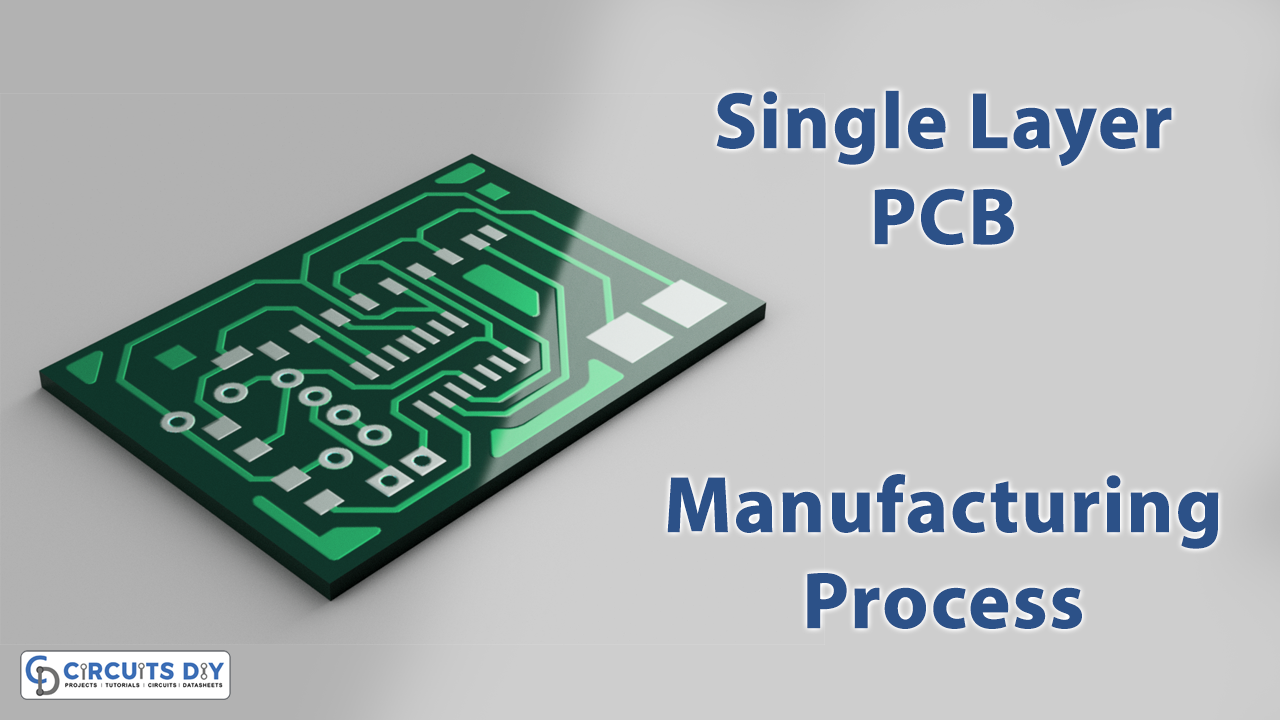
Introduction to Single-Layer PCB
If you are aware of electronics engineering you must have known about the Printed circuit boards. If not, then you must be here for exploring electronic devices and circuits. And, also for the manufacturing process. So, you have always seen green small electronic boards and thought about their manufacturing process? Those small free boards are commonly known as printed circuit boards. They are of many types. but, today we are discussing the single-layer PCB and its manufacturing process
What is Single-Layer PCB
Single-layer PCB is a PCB board having a single side of conducting material. In other words, they have just one side of the substrate to design the circuit. They are generally used in simple electronic circuits. However, they are not sufficiently promising for complex circuits. And, not effective for complicated devices

Manufacturing Process of Single-Layer PCB

To make single-layer PCBs there are various stages. Certainly, there is a whole process to design the single-layer PCB circuit. Below are the steps for making a single-layer PCB
Designing of Circuit
The first step is to design the circuit layout on the software. The software can be ORCAD, PROTEL, etc. Once the design is made, it gets rechecked if there are any errors.
Printing of the Design
The design then gets printed on paper. A special plotted printer is used for this purpose. However, the conductive areas are printed with Black ink. While clear Ink is used for none conductive areas.
Substrate Creation
The substrate is created by ironing the design on the thin PCB board. Copper is already affixed to both sides of the layers of the board. And, then etched away to illustrate the design from printed films.
Inner Layer Printing
Now, the laminate panel is covered by a photosensitive film called the resist. This resistance is made from photoreactive chemicals. This chemical gets harder after exposure to ultraviolet light.
Ultraviolet Light
The resist then passed through the ultraviolet light to get harder. This shows the pathways of copper. The excess photoresist gets removed by washing it with an alkaline solution.
Removal of Unwanted Copper
The chemical is identical to the alkaline solution is used to remove unwanted copper. And, the hardened photoresist remained unscathed.
Inspection
An optical punch device drills a pinto to keep the layers mobilized. After that, another machine inspects the board to make sure that there are no errors or flaws.
Lamination
The epoxy resin layer goes on the alignment compartment. Then a layer of substrate goes over this epoxy resin pursued by copper foil. Lastly, one more copper layer is applied.
Pressing and Drilling
To press the layer, the mechanical press is used. Then, PCB goes to laminating press which applies pressure and heat to the board. After that, holes are drilled into the layer, and the remaining copper gets removed
Plating
Now, the panel is plated with a copper layer and a thin ton guard is layered on the board. The thin tin guard is used to protect the copper.
Etching and a Solder Masking
The chemical used before removes the unwanted copper and creates the connection on board. Then the solder mask is applied. Solder mask usually involves those green color that can be seen on the PCB board. An unwanted solder mask gets removed from ultraviolet light.
Silk Screening and Surface Finishing
Silk screening prints the crucial information on board. The board gets completed by a solderable finishing that increases the quality of the board.
Testing of Board
Lastly, the designer then tested the PCB, whether it was working or needed troubleshooting. This will complete the whole process of manufacturing single layer
Related posts:
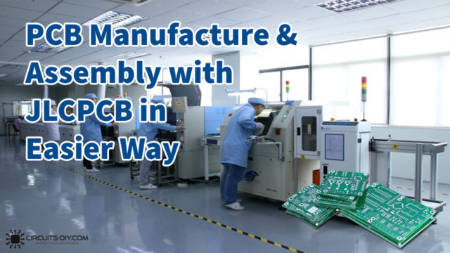 PCB Manufacture and Assembly with JLCPCB in Easier Way
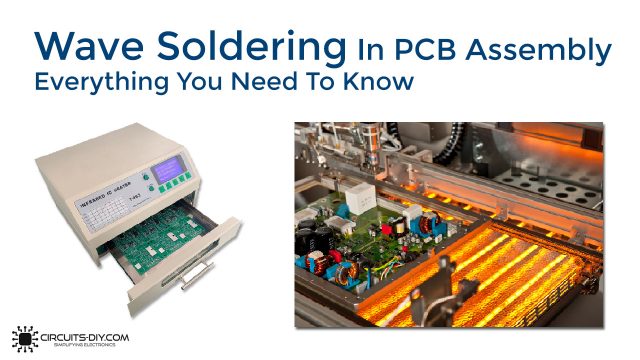 Wave Soldering Process In PCB Assembly | Everything You Need To Know
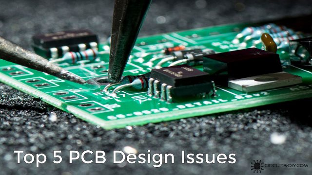 Top 5 PCB Design Issues Faced In PCB Manufacturing & Their Solutions
 Mistakes in Making of Printed Circuit Boards
 Different Types of PCB's - Printed Circuit Board
 PCB Glossary | Commonly Used Terminologies In PCB Designing