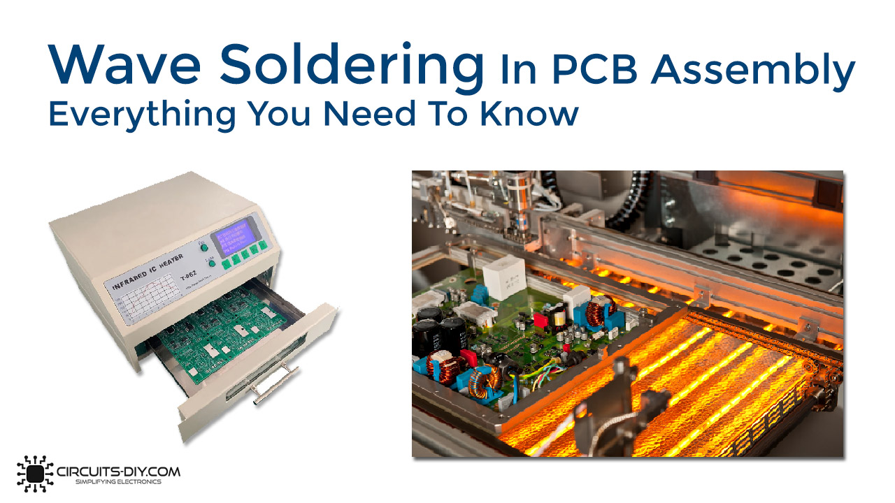
The wave soldering process is generally used for the mass production of PCBs. It allows fast soldering of PCB boards that use either or both SMDs and thin lead components. Wave soldering has become far less popular in the PCB design and assembly industry; than it was in previous years. Despite this, wave soldering remains a process that is highly effective in a number of areas, especially when the PCB assembly uses a mix of leaded and SMT components. So, in today’s tutorial, we are going to go over the PCB wave soldering process in depth; and, will also look into some of its applications.
PCB Wave Soldering Process
Wave soldering process is a meticulous soldering process in which the PCB board passes over a wave of solder. This allows the manufacturer to perform soldering in a reliable manner. This shortens the entire soldering process to mere seconds and also produces joints that can deal with high level of electrical and mechanical stress.
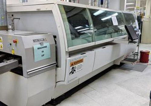
Wave Soldering Machine
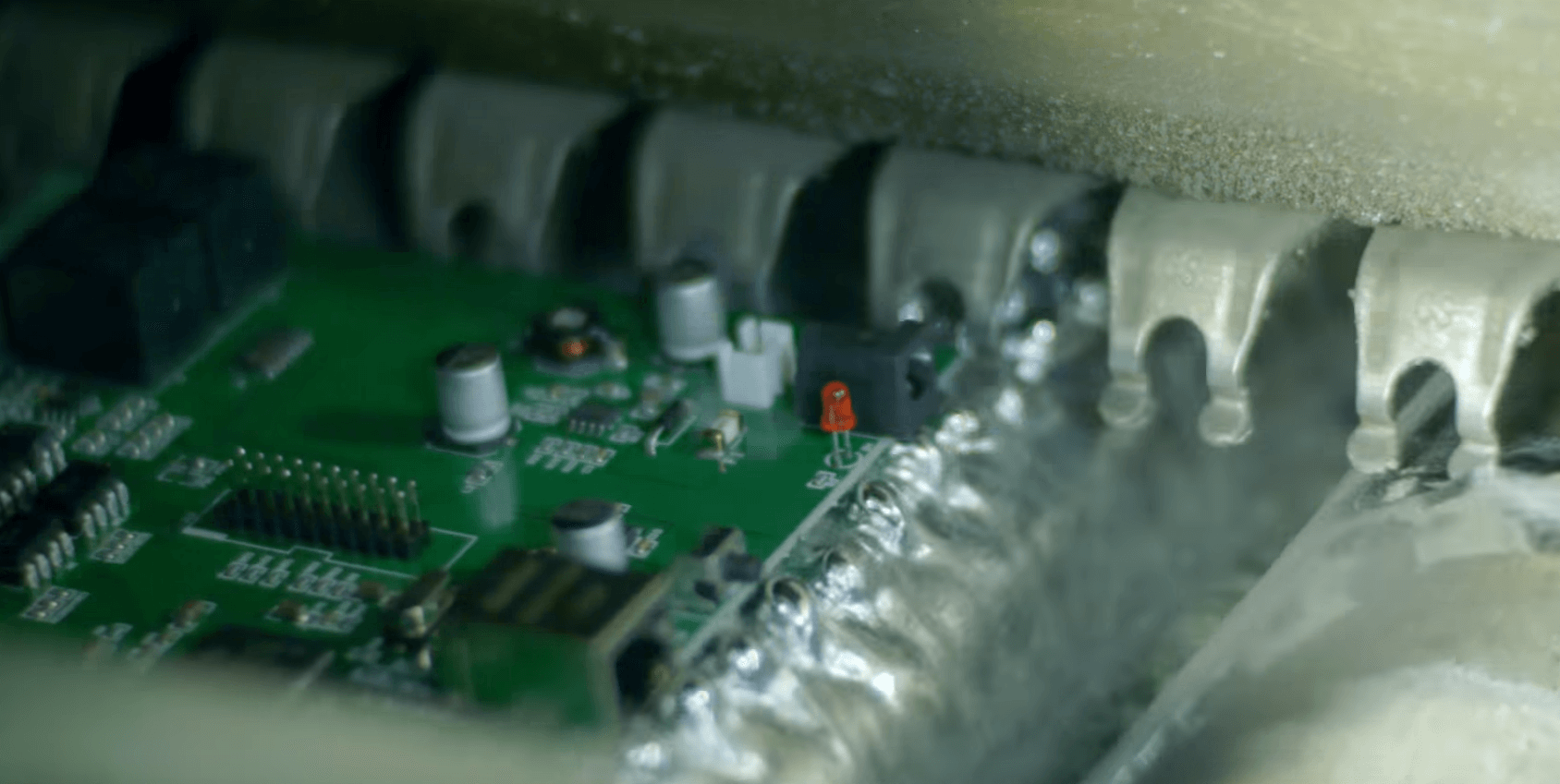
The wave soldering machine utilizes a tank to act as a vessel for molten solder paste; then, the components rolled on the PCB using a pick & place machine. After that, the loaded PCB passes over a waterfall of solder. The solder wets the exposed metallic areas of the board, creating a reliable mechanical and electrical connection.
Pre-Soldering Preparation
Solder Resist Layer
Before getting on with the soldering process, you have to make sure that a layer of solder resist or solder mask is included on the PCB board. The solder resist layer acts similar to a layer of ‘varnish’ on the PCB to which the solder paste will not stick. Don’t apply any solder resist on the area where the solder is required.

Appropriate Pad Spacing
Always make sure that there is a sufficient amount of space between the solder pads due for wave soldering process. If the solder pads are too close; then, there is a possibility of solder bridging during the soldering process, that might short the PCB board. The spacing requirements of solder pads is dependent upon the direction of the PCB board vector relative to the direction of the solder flow.

Wave Soldering Process
1) Fluxing of The Board
Fluxing of the PCB board during the wave soldering process is essential in ensuring; that, the areas on the PCB board to which the solder needs to applied are clean and free from oxidation. Flux is always on the side of the board; that is going to be in contact with the molten solder, i.e. the underside. Here, careful handling of flux quantity is imperative. Too little flux and there is a high risk of poor joints; too much flux and you run the risk of leaving greater quantities of residual flux on the board. Leaving too much residual flux on the PCB board may also contribute towards long term degradation of the PCB due to the acidic nature of the flux.
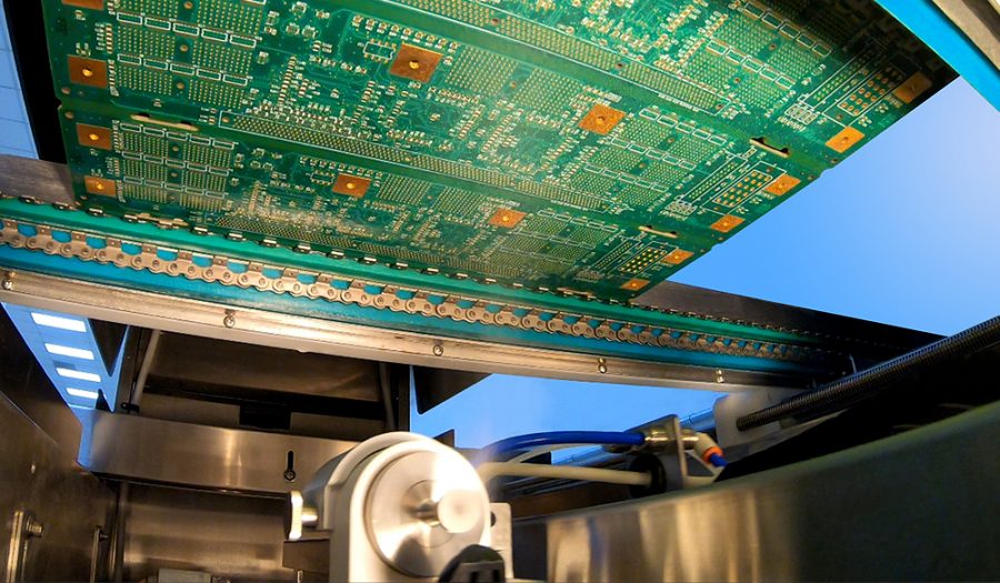
2) Pre-heat Stage
After fluxing, the PCB boards go through the wave soldering machine. Here, the heating conditions in the soldering machine exposes the board to a considerable level of heat. The preheating is fitted with hot air heaters that blow hot air onto the boards as they pass towards the wave soldering machine. On some occasions, depending upon the component density on the PCB board, IR heaters may also be used. This ensures even heat throughout the PCB board’s surface and makes sure that there are no cold spots left due to shadowing. While the pre-heating does prevent the thermal shock that the wave soldering machine would generate, the heating is also necessary to activate the flux.

Applications of Wave Soldering in PCB Assembly
PCB wave soldering has lost its popularity over the decade. The process of wave soldering is not preferred for very fine pitches required by many of the boards in manufacture today. However, it is still an ideal process for many PCB manufacturing assemblies, that use conventional lead components.
Related posts:
 6 Tips to Reduce PCB Size for Your Projects
 Advantages Of Using A PCB - Printed Circuit Board
 Double Layer PCB | Construction And Applications
 Top 6 PCB Testing Techniques Involved in PCB Manufacturing
 Laser Tripwire Security Alarm Using NE555 Timer IC
 PCB Manufacturing Process - A Complete Guide For Beginners


