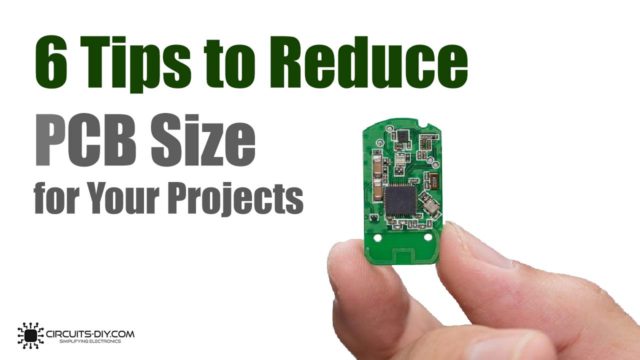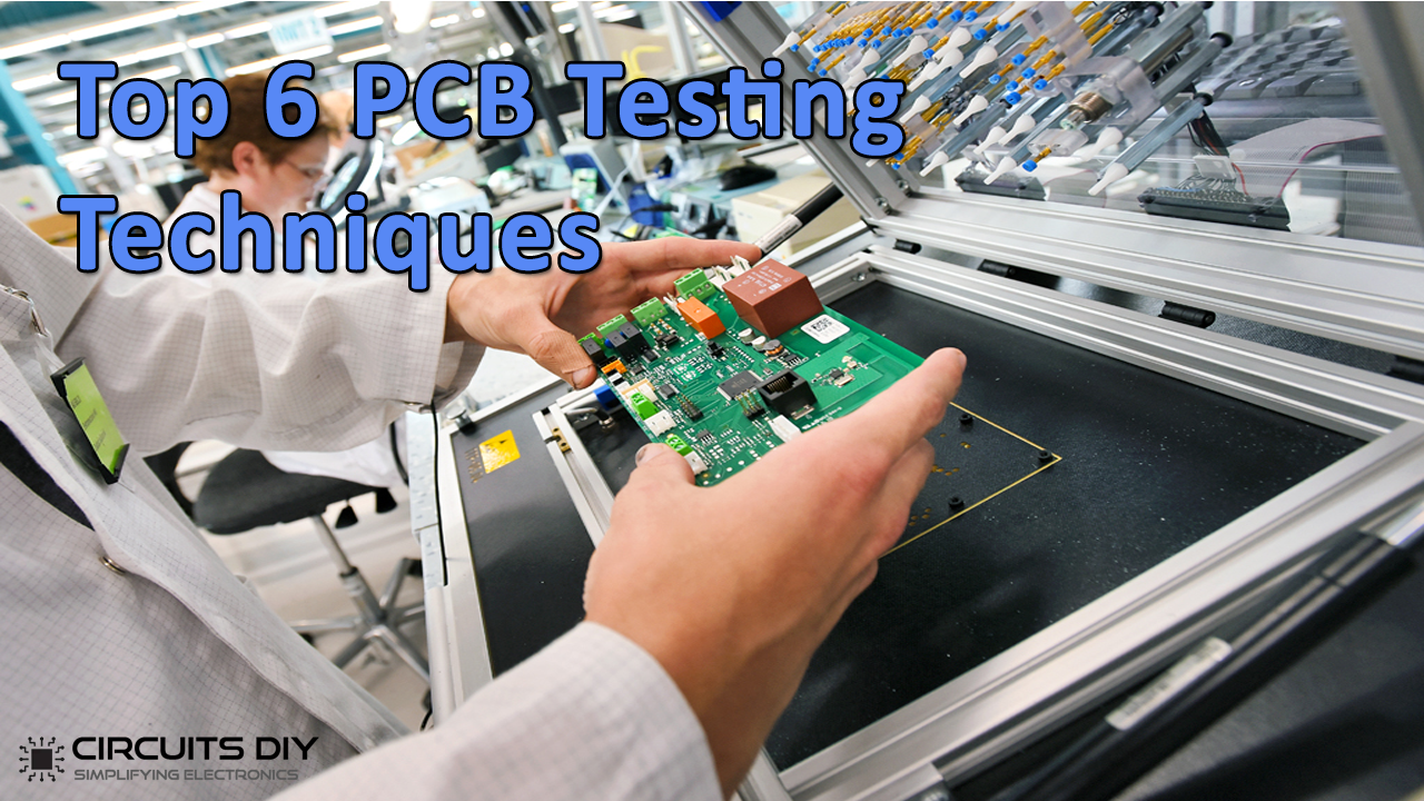
PCB design & manufacturing is an important part of today’s process industry. Nearly any industrial development cycle is incomplete without PCBs. PCB is the heart of today’s electrical industry, allowing you to connect passive/active components, and embedded devices together, into a specific form to fit the design need. So, in this tutorial, we are going to take a look into the Top 6 PCB Testing Techniques Involved in PCB Manufacturing.
PCB testing is a set of quality standards & checks on which the functionality of a PCB is judged. PCB Testing is an essential phase of PCB manufacturing. As failure in proper testing can lead to faults that may have been overlooked in the production stage. These faults may eventually result in failures & defects in the field environment. PCB manufacturing companies often have careful yet thorough testing procedures to ensure that the final PCB board is of the highest quality.

PCBWay commits to meeting the needs of its customers from different industries in terms of quality, delivery, cost-effectiveness, and any other demanding requests. As one of the most experienced PCB manufacturers in China. They pride themselves to be your best business partners as well as good friends in every aspect of your PCB needs.
Common PCB Testing Techniques
Following are the some of the PCB Testing Techniques used by most PCB manufacturers
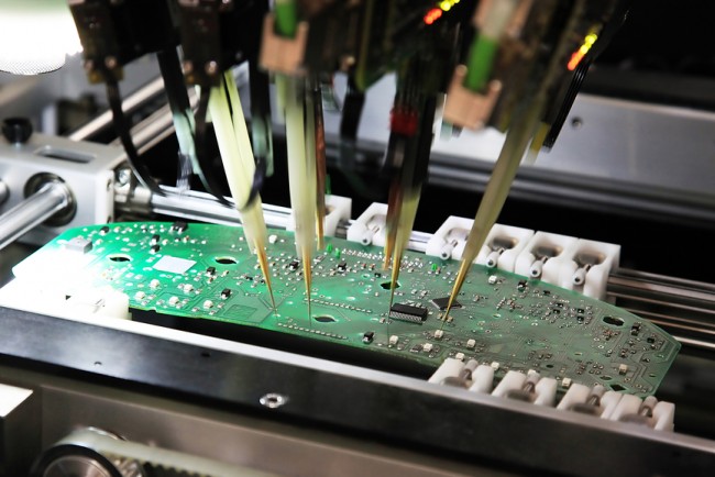
1) In-Circuit PCB Testing (ICT)
In-Circuit testing is a fully automated test, which detects defects in an assembly of PCBs through ‘Schematic verification’. ICT works in two parts, namely the Power-off & Power-on test. ICT identifies a large number of defects in the assembly which includes but is not limit to Component markings, Presence/absence of passive components, etc.
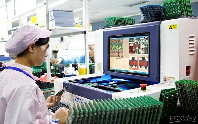
2) AOI (Automated Optical Inspection)
AOI system uses a single 2D or two 3D cameras visual input to monitor PCBs for defects. They are able to sense a variety of defects such as nodules, scratches, and stains as well as the more familiar dimensional defects such as open circuits, shorts, and thinning of the solder. AOI is very useful for the early detection of assembly issues.

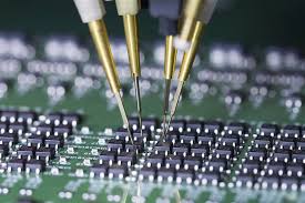
3) Flying Probe PCB Testing
The Flying Probe test is a tested & true option that is inexpensive than In-circuit testing. In contrast to the bed of nails used in ICT, this testing process uses software instructions to move electromechanical flying probes to access the PCB. It can test vias & pads to detect defects of that PCB unit.
4) X-Ray Inspection
The X-Ray or AXI can detect elements that are usually hidden from view, such as internal traces & ball grid array packages with solder joints under the chip package. There are 2D & 3D AXI tests available in today’s PCB industry, with 3D offering a faster testing period.

5) Functional Test
PCB Functional test is usually the last step in the assembly. FCT verifies a PCBs function & behavior, in various simulated field environments. Usually, the parameters of an FCT is up to the customers’ desire.
6) Burn-in PCB Testing
As the name suggests, Burn in test pushes power through your PCB card, usually to its max limit. the power is run for approx 48 to 168 hrs. If a board fails, it goes down as infant mortality. For military or medical applications, boards with high infant mortality are clearly not ideal.