
Introduction
As Electronic engineers or students, we all are aware of printed circuit boards. The printed circuit board is a major electronic component for making electronic devices and circuits. We have seen various types of printed circuit boards for various circuitry. But have you ever learned about its assembly process? In this article, we are going to discuss the PCB assembly process. This article is an overview of the assembling process using pick and place techniques for making a surface mount technology board.
Overview
The process which we are going to discuss is most familiar in the United States. PCB manufacturing is a lengthy process yet understandable. Before the technology evolved, PCBs were developed by using a soldering iron. But after some time when components get tiny it for difficult to handle with the hands. Therefore, the auto assembly process emerged.
Elements Required for PCB Assembly Process
- Centroid text files having reference designator
- Numerical control drill files
- Solder paste file
- Gerbers comprising fabrication design
Stages of PCB Assembling Process
there are several various stages of assembling PCB. However, they all are assembled to make one PCB. Every single stage is consistent with the other stage. And, this makes it easier to detect troubles that occur in the process of making PCB. Below are the stages of assembling PCB:
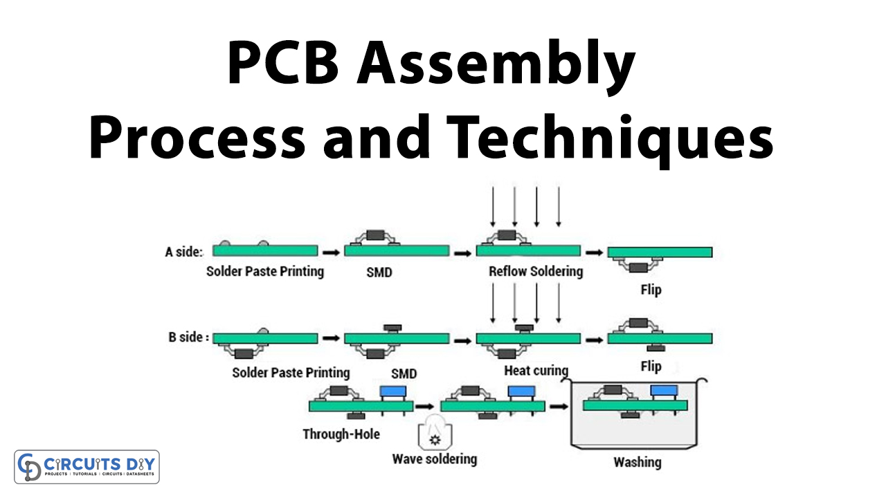
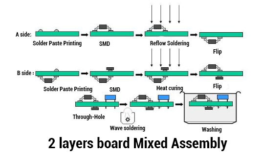
Solder Paste: It’s the most crucial step in the PCB assembly process. In every type of PCB either single, double, or multi-layer, this step remains the same for everyone. A thin metallic sheet of the stencil is placed on a board to apply the solder paste. After applying the paste, the stencil is cleared out.
Pick and Place: The automated or robotic machine picks and places the components in a surface mount technology. On the other side, through-the-hole technology utilizes the manual method.
Soldering: To join the components on the PCB board wondering is a necessary step. Through-hole technology uses the wave soldering method. However, surface mount technology uses the reflow method. Consequently, PCB is going through to a 50-degree Fahrenheit of temperature.
Inspection: Inspection is mandatory to assure the functioning of the design circuit. There are given the three main methods of inspection:
- Visual Inspection: It’s a manual method of inspection. The method is only favorable for small PCBs
- Automatic Optical Inspection: This method uses high-resolution cameras, aligned at several angles. This method is useful for single or double-layer PCBs
- X-Ray Inspection: This method is practical for multi-layer PCBs. Because these PCBs are difficult to inspect in the prior above methods
Functional Testing: After all those stages, the last step is the post Assembly inspection. However, Functional testing. requires numerous ways. The process detects if there are any problems in the building of the PCB.
Conclusion
In short, PCBs require so many different yet simple stages for it’s assembling. These steps are fundamental to making a circuit on PCB. These steps require a little attention. However, it makes the device more worthy to use.
Related posts:
 PCB Design Issues Faced In PCB Manufacturing & Their Troubleshooting
 Build Your Private Online Parts Warehouse in JLCPCB
 Single-Layer PCB Manufacturing Process
 Top 6 PCB Testing Techniques Involved in PCB Manufacturing
 PCB Component Placement Guidelines - Tips & Tricks
 Manufacture your Multilayer PCB at Cheap Prices from JLCPCB


