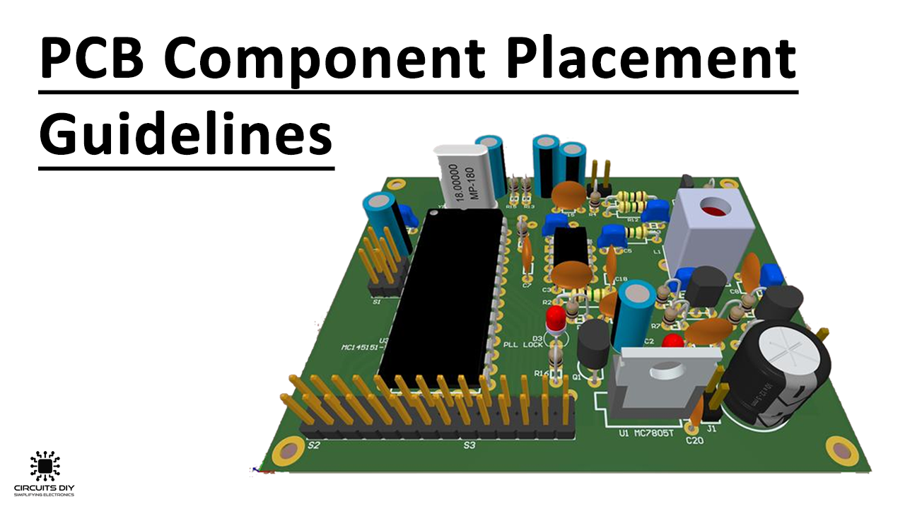
PCB designing is both an art and a science. There’s a ton of technical know-how and measurements to consider when dealing with trace widths, layer stack-ups, schematics, etc. When you get to the artistic side of PCB design with component placement, and this is where things get interesting. There’s a common saying that – PCB design is 90% placement and 10% routing. This is entirely accurate. Taking the time to precisely place your components will make your life a whole lot easier, when it comes time to route everything, while also giving your board its best electrical performance.
Basic Component Placement Guidelines to Consider
The majority of component placement problems that affect manufacturing are when components are placed too close to the edge of the board. This potentially can result in damage to the board from different sources, such as automated assembly equipment during a volume manufacturing run. Given below are some other placement considerations that you should keep in mind:
- Place your fixed parts first. These parts include anything that has to interface with the rest of the system that your board is going to be used in for example Connectors, switches, etc. Mechanical parts such as nuts and bolts will also need to be placed in fixed locations. Before placing a part down, you should also know exactly where your mounting holes and edge connectors should go and what kind of mechanical enclosure to fit your board.
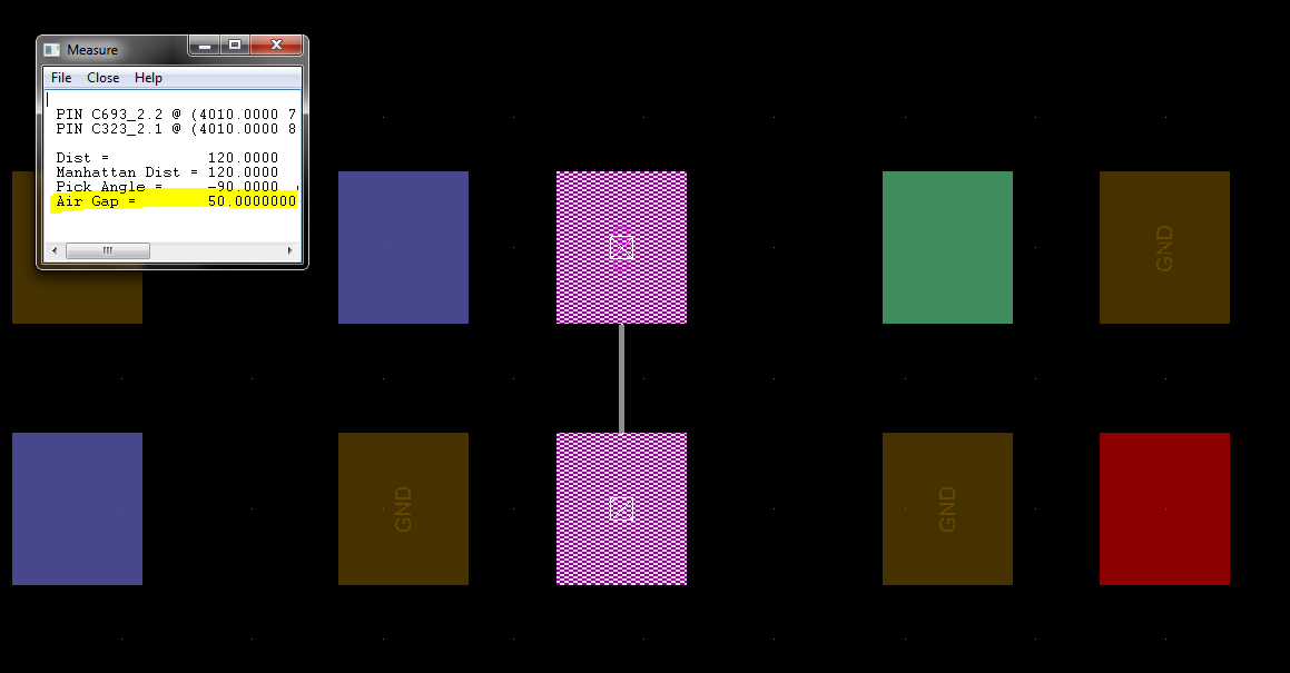
- Components placed too close together could cause problems for automated pick-and-place machines during assembly and for testing. Keep at least 50mil space between components and 100mil space from component to board edge. Place connectors on one edge or on one corner of the board.
- Try to place all components on the top side of the PCB. If not possible, only place small size and low thermal dissipation components (like SMD passive parts) can be on the bottom side.
- For groups of similar components place them in the same direction in evenly arranged rows or columns.
- Place decoupling capacitors as close as possible to VCC pin on active components.
- Always try to leave at least 350 – 500mil space between each integrated circuit (IC) on your board. For larger ICs you have to leave even more space.
- Discrete components should be placed such that both pins enter the solder simultaneously when the board goes through the wave soldering. Larger parts should not precede smaller parts to avoid shadowing, which could cause insufficient solder joints between component pins and their metal pads on the board.
Conclusion
When you place your components, keep in mind that your PCB design tools have a lot of functionality built-in that might be helpful for you. There will be different placement utilities to use, as well as the ability to change the display in order to help you organize and place your board. The best PCB layouts started on a foundation of great component placement, so you should not rush through this process. If you find yourself spending 90% of your time placing parts, then you’re doing great. This process is a rewarding creative endeavor, and probably one of the most challenging aspects of the PCB design process that you’ll wrestle with, but it’s totally worth it.