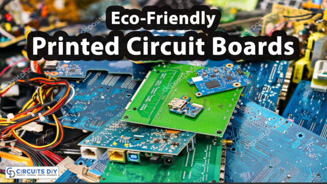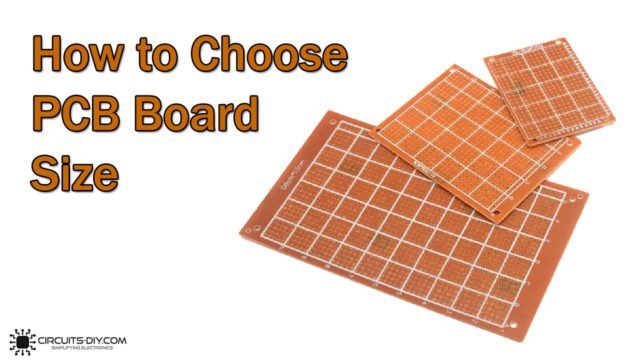
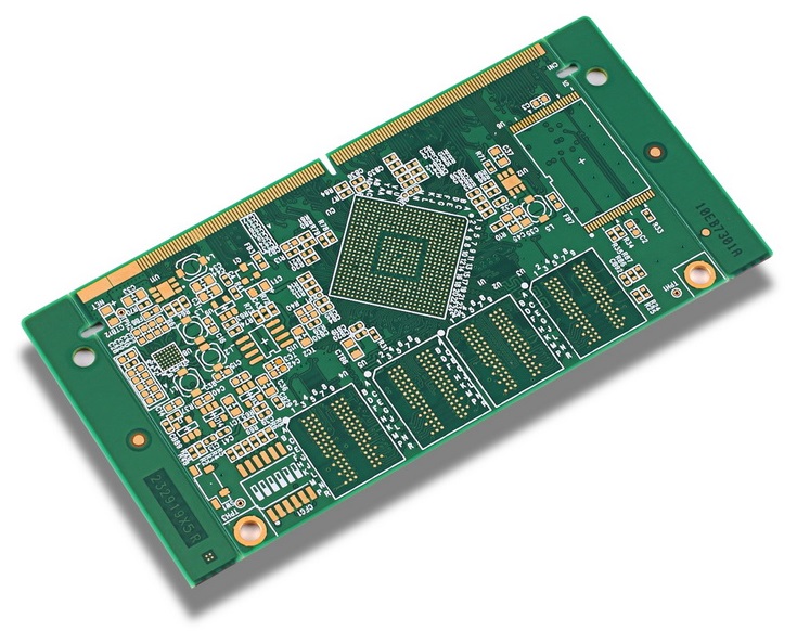
Introduction- PCB Sizes
Different electronic devices have different sizes. Therefore, the size of PCB is diverse for different electronic circuits. The PCBs in our computers are larger. However, the PCBs in smartphones are smaller. Since we are living in the technological era, where human wants everything to be light and tiny. Hence, designers work every day to reduce the size of PCB. So that it may reduce the size of the devices. So in this article, we will try to explore how to reduce the size of PCB for electronic devices.
It’s considered complicated and tricky to reduce the size of the PCB. Because it depends on the various factors. And that’s why it has some limitations. Following are some of the techniques to lessen the size
JLCPCB is the foremost PCB prototype & manufacturing company in china, providing us with the best service we have ever experienced regarding (Quality, Price Service & Time).
6 Important Tips
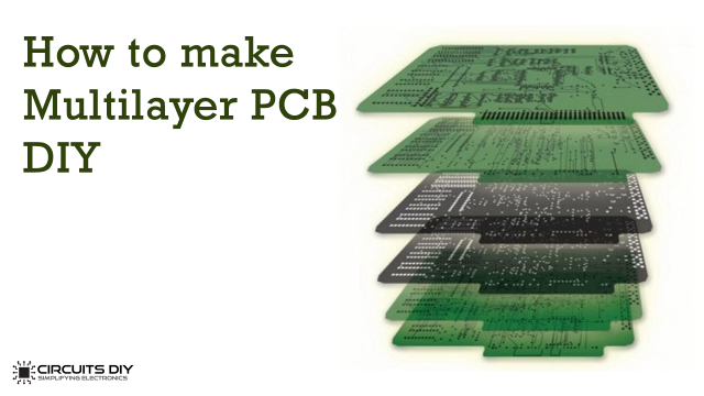
(1) Use of Multi-layer PCB
Usually, multi-layer PCBs are complex and difficult to handle. But, it can reduce the device size by assembling the whole circuit on a single PCB. Since the making of the multilayer is difficult. Therefore, a designer can use a technique to first make a prototype on a single or double-layer PCB and then when gets satisfied after testing, assemble it on a multi-layer. This can make work easy, and also reduces the PCB size. In other words, device size decreases.
(2) Increase Copper Thickness
When the high current flows through the circuits on PCB. This transfers more heat into the circuit. Now, it is necessary to manage thermal issues. So, heat sinks are used for this purpose. But this increases the size of the PCB. To shrink the board size, use thick copper layers. Thick traces can easily manage high current and heat dissipation. Also, then there would be no heat sinks required. Hence, decreases the size of PCB

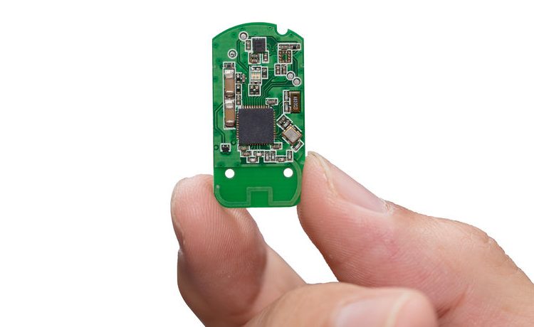
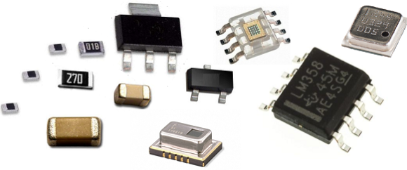
(3) Select Smaller Components
Most of the designer uses large resistors like 0805 or 1210 and none polarized capacitors. Because they are manageable and easier to handle. But, at the same time, it takes the huge on the board. So, it is recommended that to use the components having smaller sizes with the same rating. Remember, some of the smaller components can’t handle higher currents. So, be careful while selecting.
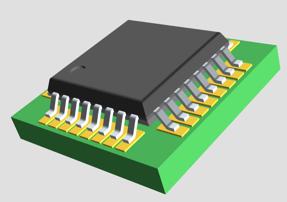
(4) Use Compact Connectors
Connectors take a lot of space on the PCB board. But there are some promising manufacturing companies out there providing different sizes of connectors. Selecting the right size can solve the problem
(5) Decreasing the Foot Prints
The default footprints for the components in the circuit are bigger than you need. This increases the size. Select the footprints by checking the datasheet of your required component that how much space you actually needed for that. Then, try to modify the design according to it. This may help to reduce or shrink the PCB of your project.
(6) Use stacked Packages
The standard packages require more components. Like if you’re adding the resistors in series or parallel to make a specific resistance. Then try to use that resistor having that particular resistance instead of using many small resistors. In the same way, use one big capacitor instead of many small capacitors. This could be done for every component.