The use and need for printed circuit boards have seen a rapid increase in the past few decades. With the ever-reducing technology size and the constant increase in design complexity, it has become ever so necessary to innovate and implement PCBs that are accommodating and keep up with the rising design needs. Single-layer PCBs have been the general preference for PCB designing and assembly, but the evolving design industry indicates an increasing need for PCBs that can house a large no. of components without requiring extra clearance. Double-layer PCBs offer a definitive and cost-effective solution to this problem. So, in today’s guide, we will cover Double-layer PCBs fully, going over their construction and applications in the electronics industry.
What is a Double Layer PCB?
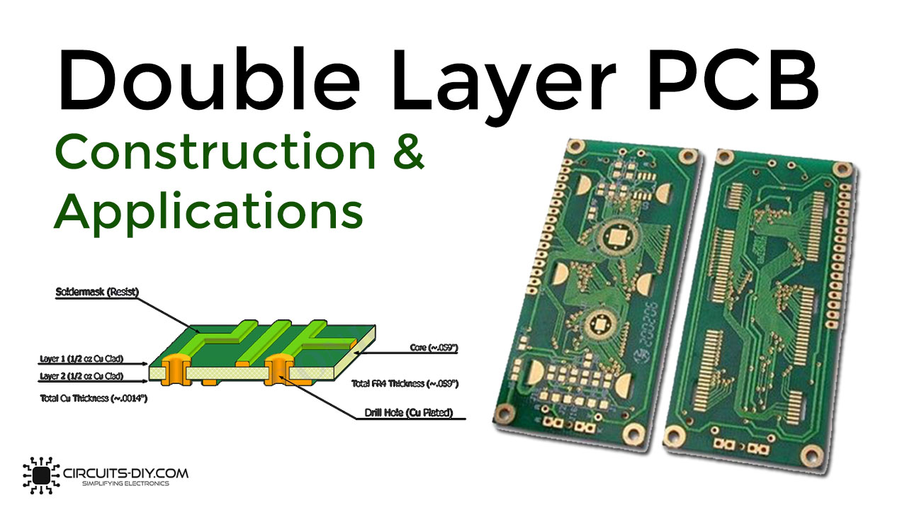
A Double Layer PCB or a double-sided PCB is a thin layer of directing material, similar to copper, connected to both the best and base sides of the board. It is extremely useful in many electronic applications because circuits on one side of the board can be connected on the other side of the board with the help of holes drilled on the board.
Structure of a Double Layer PCB
The structure of a basic Double-layer PCB is as follows:
Pad:
The Double-sided PCB padding is only a small bit of copper connected to which are the legs or leads of the parts. The legs are usually bounded with the pads using solder.
Trace:
They are simple copper metal busses used to connect PCB parts and legs with each other.
Silk layer:
The silk layer is utilized for printing lines, content, or any workmanship on the surface of the PCB. For the most part, for screen printing epoxy ink is utilized. Silk layer can be utilized as a part of the best or potentially base layer of PCB as indicated by client necessity which is known as silkscreen TOP and silkscreen BOTTOM

Top and Bottom layer:
In the Top layer of PCB, all segments have mounted this layer of PCB. For the most part, this layer is green-shaded. In the base layer of PCB, all segments are fastened through the opening, and the lead of segments is known as the base layer of PCB. At some point, at the top of the potentially base layer, PCB is covered with a green shading layer, which is known as a weld veil.

Solder Mask:
There is one additional layer on the top of the copper layer called Solder Mask. This layer generally has green color but it can be of any color. This insulating layer is used to prevent accidental contact of pads with other conductive material on PCB.

Applications of Double Layer PCB
Medical Devices
Double Layer PCBs have a significant contribution to the medical industry. Not only they are used in medical devices but they also play an important role in diagnostics, testing, and monitoring.
Automotive Uses
The use of double-layer PCB in the automotive industry allows engineers to feature new electronic features such as better GPS systems and entertainment systems. It also allows them to update or enhance any existing systems due to the easy interchangeability offered by double-layer PCB boards.
Consumer Electronics
Consumer electronics is perhaps the domain in which double layer PCBs are most abundantly utilized. Due to the massive amount of electronics innovated and designed every year, the demand for double-sided PCBs is also increasing. Double layer PCBs are used in consumer electronic applications such as mobiles, laptops, kitchen appliances, LEDs, etc.

Industrial Electronics
Double-layer PCB is required for high-power applications as well. Double-sided PCBs manufactured from high-grade materials are readily utilized in industry. These kinds of PCBs must be able to survive harsh conditions such as harsh chemicals, vibrating machinery, and rough handling.
Related posts:
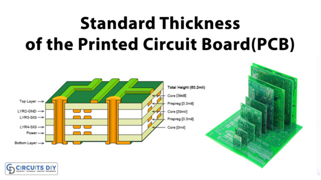 Standard Thickness of the Printed Circuit Board(PCB)
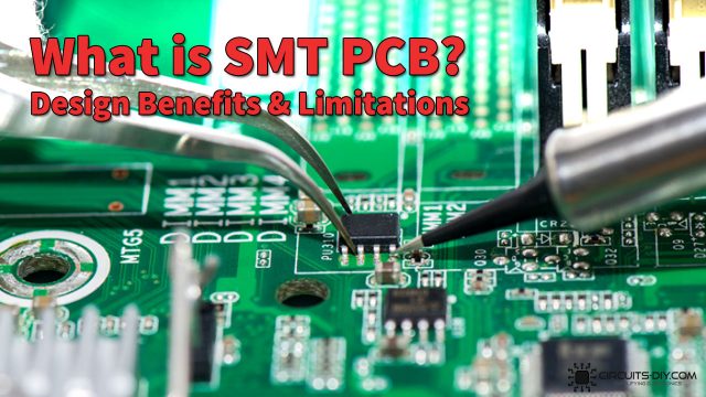 What is SMT PCB? | Design Benefits and Limitations of Using SMT PCBA
 Printed Circuit Boards Assembly Overview- Steps and Process
 Cost-saving tips for PCB Fabrication
 How To Make A Multilayer PCB At Home - A Beginners Guide
 Ordering PCB | 5 Reasons Why Not to Order PCBs Through PCB Brokers


