Introduction
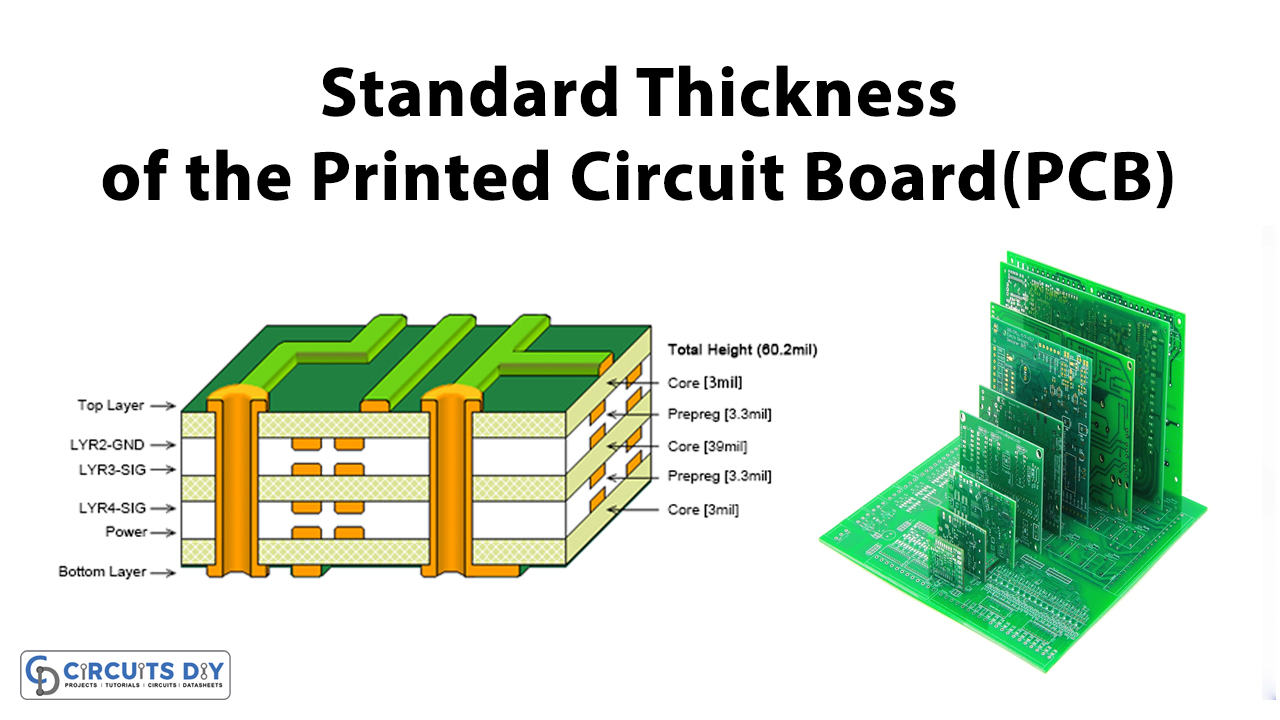
While making electronic circuits, there are many factors that a designer must have to consider. One of the most important factors is the thickness of the printed circuit board (PCB). Hence, the thickness can be estimated through different parameters. The typical way to determine the overall thickness is through the layers of the PCB. Now, PCB comes in 2 to 32 layers, therefore it is sizeable and difficult to cover the standard thickness. However, it is crucial to determine the thickness, as it affects the mechanical weight, influences the conductivity, and changes the resistivity accordingly. In short, PCB thickness plays an important role in the functionality of PCB.
Standard Thickness of Printed Circuit Board
Printed circuit board(PCB) thickness was defined in the 20th century when PCBs have a single panel with several layers placed together. Thus, the standard thickness is 0.063 inches. This was basically determined through the substrate used previously. The plywood substrate has a thickness of 0.063 inches. Therefore it becomes the standard thickness. But, modern PCBs are either of a single copper layer or multilayer that have substrate between them. As a result, the board thicknesses can be in the range from 0.008 inches to 0.240 inches. However, some factors estimate the overall thickness of the board. And, these are:
- Board thickness
- Copper thickness
- trace thickness
PCB Board thickness
The thickness of the board depends on the material used in the boards. Earlier the standard thickness was about 0.0065 inches because of the substrate that is used between the copper foil. Concerning time, when the lighter substrate got introduced, the size also gets decreased. Now, the modern PCB boards use substrates like epoxy, resin, etc instead of plywood. Therefore, the size of the board thickness can be below 0.0065 inches.
Copper Thickness of PCB
The thickness of the copper plays an essential role in the thickness of the overall thickness. The standard copper thickness is 1 once. Hence, obtained by spreading this ounce of copper uniformly over the square foot area. But, there are circuits where the current requires more thickness. In those conditions, the copper has been added accordingly. However, the process requires time and is very challenging.
Trace Thickness of Printed Circuit Board

Trace thickness is specified by the designer and is written in the Gerber file. trace thickness should be strong enough to bear the coming amount of current without any damage to PCB. In other words, it must acknowledge a higher fraction of current without changing the average temperature of the PCB. The task to define the trace thickness is difficult. Therefore, designers use a PCB width calculator for this purpose. The calculator determines the appropriate trace thickness that can pass the amount of current needed for the circuit without doing any damage to the PCB.
Conclusion
Printed circuit board functioning profoundly depends on the thickness of the board. And, the overall thickness of the board can be estimated through three main parameters that we have discussed above. Thus, every three-parameter has its own thickness that helps to measure the overall thickness of the board. Usually, the boards’ thickness is 0.063 inches which are widely in different electronic devices.
Related posts:
 PCB Cleaning Solutions 101 | Ultimate Guide To Keep Your PCB Clean
 Saving Time And Money In PCB Manufacturing | Five Golden Rules
 Printed Circuit Board Grounding Tips and Techniques
 Black Printed Circuit Board | Design Benefits And Limitations
 Mistakes to avoid in the PCB Design Process
 Ordering Cheap PCB 2$ PCB Prototype


