
Introduction
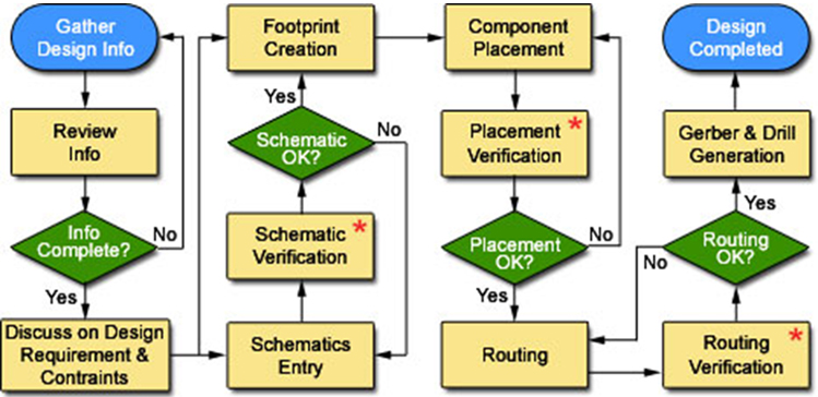
A PCB-making process is enormous. But, a single mistake in the process can affect the entire PCB. The process includes so many steps. And, every step should be completed effectively and adequately. To make an error-free PCB, a designer must have to design the circuit by avoiding mistakes. But what are these mistakes? So, here are some common mistakes to avoid in PCB designing. Some common mistakes are described below:

• Wrong Tools in the making of PCB
Wrong tools can make the device worst. Tools include schematic software, equipment, and also stencils. The wrong tool can make an insufficient design. Moreover, it may increase the cost of the circuit. So, it is always preferable to use the best tool available. Do proper research and analyze what tools are promising for your project
• Ineffective PCB Layout Technique
If you do not select the proper layout board technique, it may risk your device. Since many of the components are near to each other. So, there can be a danger of connection. And, sometimes designers are working on complex circuits. Therefore, it is necessary to avoid this mistake.
• Incorrect Thickness of Copper
PCB having different types needs a different kind of possible thickness. A circuit designer must be specific about the parameters. Many designers use an ounce of copper. This is not sufficient for the board. This results, inadequate plating in the holes. So, it is recommended to use 1 it 2 ounces per square ft.
• Inaccurate Assembling of the Decoupling capacitor
Decoupling capacitors are placed on the power supply rail for a stable voltage source. But, some designers make mistakes and do not place them close to the pin that requires a stable voltage which can cause damage. . Also, it is important to place the output capacitor close to the output pin of the regulator.
• No Testing or Review
To avoid errors and mistakes, the designers must test their designs on the prototype Before connecting to the device it is useful to test the design practically. It may also help to save the device from any damage. Also, designers must need to review if find any errors. In that case, a review of the schematic layout of the software would be the first step.
• Lack of Communication
The team must need to communicate. While working on a large project, stress is the major issue. And, designers start multitasking. This results in low productivity and can build inefficient PCBs. Therefore, members of the team must need to divide the work accordingly. And, together make the achievable timeline to complete the PCB. This would help to give more motivation and a better product in the end.
Conclusion
By avoiding above mentioned mistakes, a designer can design an efficient, valuable, and reliable product. And, this can also increase the durability rate of the device. In the other words, it would give large life to the device or the PCB. The designer must need to know these mistakes to make an effective PCB. Do you know some more Mistakes to avoid in the PCB? Write it down in the comment section.
Related posts:
 How Does the PCB Assembly Process Work?
 PCB Soldering Techniques & Best Practices For Absolute Beginners
 What is SMT PCB? | Design Benefits and Limitations of Using SMT PCBA
 Multi-Layer PCB Applications & Advantages
 High Speed Printed Circuit Board Design Tips
 PCB Manufacturing Process - A Complete Guide For Beginners


