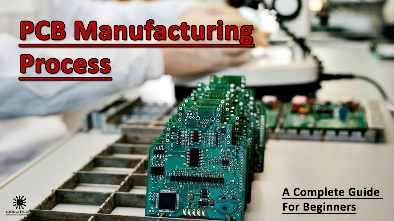
The PCB design & manufacturing process is very crucial for anyone in the electronics industry as PCBs are basically the basis of all electronics circuits functioning in today’s world. With the rapid increase of pace in the world of electronics, PCB technology is also seeing a huge influence in terms of Track size reduction, increase in PCB layer & complexity to accommodate for the increased connectivity, and improved design rules to ensure that smaller SMT devices can be handled and the soldering processes used in production can be accommodated. So, In this article, we are going to go over a complete Beginners Guide To The PCB Manufacturing process.
PCB Manufacturing process is basically a string of industrial design steps, essential for efficient mass production of PCBs while ensuring the quality of design & minimizing the risk of troubleshooting.
JLCPCB is the foremost PCB prototype & manufacturing company in china, providing us with the best service we have ever experienced regarding (Quality, Price Service & Time).
Basic Integrants Of A PCB
Today Printed Circuit Boards can be made from a wide variety of substances. The most commonly used is a form of glass fiber-based substrate known as FR4 epoxy glass board. This provides a reasonable degree of stability under high stress & temperature and doesn’t break down badly. Other cheaper materials are readily available for PCBs in low-cost commercial products such as PTFE based printed circuit boards.
How is a PCB Manufactured?
Following are the common steps for the PCB manufacturing process:
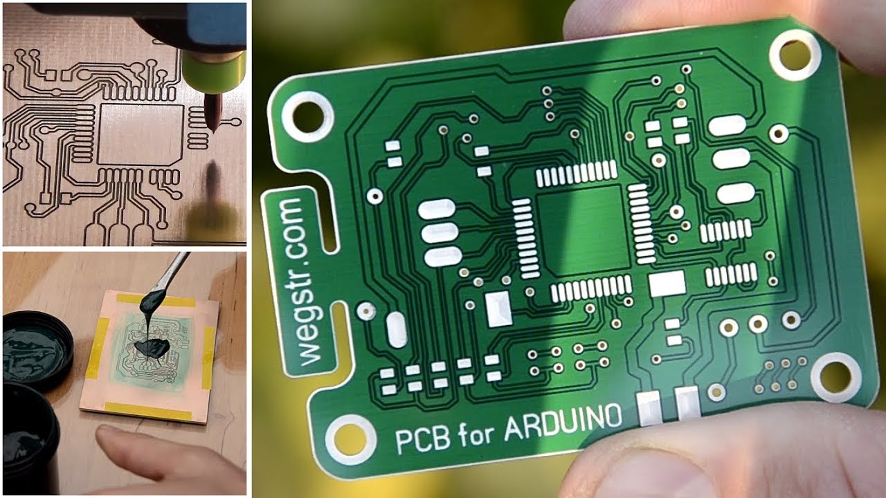
Step 1: Designing & Printing the PCB Design
The start of any manufacturing process for any kind of PCB starts of course with the design & printing phase. The designer layouts the initial schematic of the PCB, outlining all the fulfilled requirements using design software such as EasyEDA. After examination, the PCB design goes to a PCB fabrication house. On arrival, the PCB design plan undergoes a second check, known as a Design for Manufacture (DFM) check. After the checks are complete, the PCB design can be printed using a plotter printer. After the film is printed, they’re lined up and a hole, known as a registration hole, is punched through them.

Step 2: Printing the copper for the Interior Layers
The PCB design is then printed onto a piece of laminate. Copper is then pre-bonded to that same piece of laminate, which serves as the structure for the PCB. The copper is then etched away to reveal the PCB design from earlier. Next, the laminate panel is covered by a type of photo-sensitive film called the resist. The resist allows technicians to get a match between the photos of the blueprint and what’s printed to the photoresist. When the resists & the laminate lineups perfectly they get expose to UV light. The UV light passes through the translucent parts of the film, hardening the photoresist. This indicates areas of copper that are meant to be kept as pathways while black ink serves as a prevention for blocking light from getting into areas not meant to be hardened.
Step 3: Removal of Unneeded Copper
The next stage in PCB fabrication is getting rid of unwanted copper. After cleansing the board with an alkaline solution, the board goes through a wash of another powerful chemical to eat away at the copper that the photoresist is not covering. Once the unprotected copper is removed, the hardened photoresist from earlier also needs to be removed, leaving only the copper necessary for the PCB.
Step 4: Inspection & Layer Alignment
After cleaning, Each PCB goes through layer alignment and optical inspection. To align the layers, they go through a type of punch machine known as an optical punch. The optical punch drives a pin down through the holes to line up the layers of the PCB. Following this step, another machine performs an optical inspection to make sure there are no defects. This optical inspection is important because once the layers are in a strong fix together, there is no chance to change any errors that may exist.
Step 5: Laminating the PCB Layers
The next step is the laminating of the PCB layers, which is in two stages:
Lay up Step:
In this step, a layer epoxy resin & a thin layer of copper foil covers the inner and outer layer of the PCB. The foil contains the etchings of the copper layer. Once the outer &inner layers are ready, they are sandwich together using metal clamps on a press table.
Laminating Step:
This step begins by placing a layer of epoxy resin on the alignment basin of the table. A layer of the substrate covers the pre-impreg resin, followed by a layer of copper foil. After checking the copper foil, a technician takes it over to a press and presses the layers down and together, punching down pins through the stack layers, ensuring the stacking stability. After this, the layers go through a laminating press, melting the epoxy inside of the prepeg, the heat of the laminating plates, and the pressure from the press combine to fuse the stack of PCB layers together.
Step 6: Drilling
In this step, a technician drills the guiding holes using a drill machine, so that the PCB is secure before the drilling of design specific holes. When it is time to drill these holes, a CNC drill makes the holes itself, using the Gerber file as a guide. Once the drilling is complete, a filer files of any additional copper from the edges of the board.

Step 7: PCB Plating
in this step, a chemical fuses all the different layers of the PCB together. After cleaning, the PCB is bathe in a series of chemicals. Part of this bathing process covers the panel in a micron-thick layer of copper, which deposits over the top-most layer and into the holes.
Step 8: Imaging & Plating the Outer layer
In this step, a coat of photoresist covers the outer layer of the PCB and go through imaging. Then, they go through the plating process in the exact same way the interior layers of the PCB in the previous step.
Step 9: The Last Etch
In this step, the out layer of the PCB goes through one last etch. Here, the tin guard helps to protect the copper during the etching process. After removing all undesirable copper & establishing all PCB connections. the PCB is ready for solder masking.
Step 10: Solder Mask
In this step of PCB Manufacturing, an ink epoxy along with a solder mask film covers the PCB board. after this, the PCB boards go through UV ray exposure to mark out certain portions of the solder mask for removal.
Step 11: Finishing & Silk Screening
As part of the finishing process, the PCB is plated with gold, silver, or HASL so the components are able to be soldered to the pads created and to protect the copper. After this, it is silk-screened. The silk-screening process prints all of the vital information on the PCB, such as manufacturer marks, company ID numbers, and warning labels.
Step 12: Functional Reliability Testing
In this step, the PCB goes through a battery of electrical & functional tests. The most important test to perform are the continuity test & the isolation test. While the electrical tests mainly exist to ensure functionality, they also work as a test of how well the initial PCB design stood up to the manufacturing process.

The final PCB board goes through one last inspection phase. Here, checks for general cleanliness are ran to ensure that there are no sharp edges, burrs, or other manufacturing hazards. Also, checks for Slots, chamfers, bevels, and countersinks are ran as per client specifications.
Related posts:
 All about Aluminum PCBs
 Gerber Files Explained: Their Role & Need in PCB Manufacturing
 Do's & Dont's of PCB Designing - Tips & Best Practices
 Why More and More Customers Choose JLCPCB PCBA one-stop service?
 PCB Cleaning 101 | Top Methods to Keep Your PCB Spotless
 How to make 1$ DIY PCB Holder - Circuit Board Holder


