PCB layout designing is integral to the PCB fabrication process. Most young engineers step into the PCB industry with no prior knowledge on good layout practices, also professional engineers have bad habits that derive from old manufacturing processes. The consequence of a bad PCB design is very inflicting, your design will not be legally sold if it does not pass the appropriate test associated with your industry. So, in this article, we will go over the top 5 Do’s & Dont’s of PCB Designing that you should employ in your everyday design practices to boost production efficiency.
Proper PCB designing requires a number factors to be taken care of, these factor include parameters ranging from proper organization to proper design protocols. In this article, we are going to look into some of the key Do’s & Dont’ you should consider while designing your next PCB project.
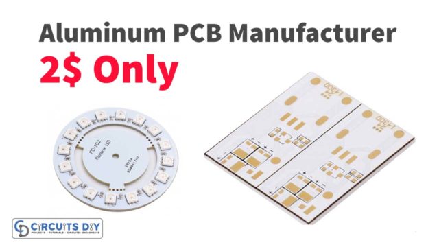
JLCPCB is the foremost PCB prototype & manufacturing company in china, providing us with the best service we have ever experienced regarding (Quality, Price Service & Time).
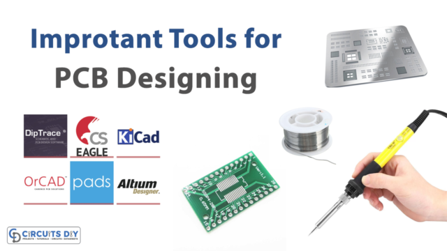
1) Choose the Correct Design Software
Perhaps the most important step in proper PCB design is to choose a design software that caters to all your design needs. The tool that you use to design your boards should at least minimally meet the essential feature requirements present for your design. I must recommend using easyEDA it’s really simple and easy to use as its name implies.
2) Ensure Design & Drawing Match
Mismatches in Design & Drawing can cause major malfunctions & delays in the final production phase of the PCB. So, be sure to check for things such as drawing to data dimensions, hole quantity, pad size, and revision levels. The take-away from this is to always double-check your designs with respect to the initial schematic.
3) Incorrect Antenna Layout
While designing PCB schematics for wireless devices such as RF transceivers & RFID tags. The layout of the antenna on the PCB is crucial and is usually layed out incorrectly, even by the most competent engineers. For max power transfer between the transceiver and the antenna, you must match their impedance. This means their complex impedance and not their simple resistance. You’ll need a proper transmission line to connect the antenna and the transceiver. Most of the time, the transmission line should have 50 Ohm impedance for max power transfer with the antenna.

4) Thermal Vias
Vias move heat from one side of a PCB to the other. Large vias transfer heat more efficiently than small vias. Using numerous vias into your design scheme transfer heat more efficiently than one via, and lower the operating temperature of components. Lower operating temperatures contribute to higher reliability.

5) Use Small Loops
Loops, especially high frequency loops, should be made as small as possible. Small loops have lower inductance and Ohmic resistance. Placing loops over a ground plane further reduces inductance. Having small loops also reduces high-frequency voltage spikes.

6) Concurrent Engineering Services
If you are unsure about the reliability of your design or if you need a pro’s opinion, be sure to use PCB design services such as JLCPCB. Having a second opinion is always useful in ensuring your designs functional success.