Introduction
PCB boards are regarded as a crucial and dependable component of all electronic products and projects. It is now the greatest and finest tool for creating projects and connecting their many parts. Making printed circuit boards is a difficult task that requires much thought, hard work, and energy. A single PCB must go through a variety of manufacturing procedures. From drilling to etching, from outer layer inspection to solder mask coating, and from final cleaning to fabrication, we have you covered. As a result, patience and time are required. It becomes challenging for a typical designer to perform all this while creating more designs. As a result, manufacturers like JLCPCB make things easier by offering low-cost, high-quality, efficient PCB manufacturing and assembly, making them appealing. Here in this article, we will see the JLCPCB Manufacturing and Assembly Capabilities
China-based PCB manufacturing company JLCPCB is the most dependable and trustworthy PCB provider with top-notch, knowledgeable engineering staff. For the past 15 years, they have been providing their clients with high-quality PCB boards, assembly services, and on-time delivery.
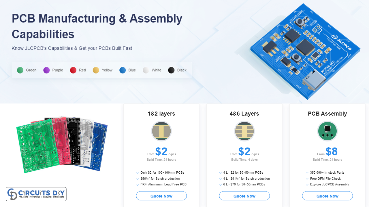
JLCPCB Manufacturing and Assembly Capabilities
Here are some of the capabilities of the JLCPCB Assembly
For Economic PCB Assembly
Assembly Types
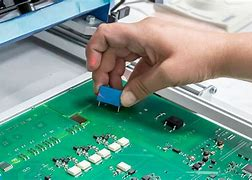
- Single-sided placement (SMT/Thru-hole)
Surface-mounting assembly SMT is a type of assembly that involves soldering surface-mount components on PCBs.

Electronic circuits are built for through-hole PCB assembly so that the components may be simply drilled or passed through the pre-drilled or already-drilled hole into the PCB.
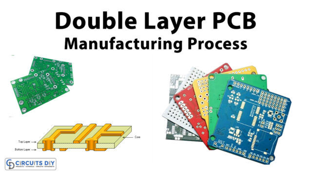
PCB Layer
- 2,4,6 layers
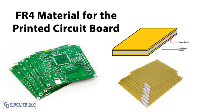
A PCB is built on layers. They, therefore, consist of copper, a dielectric, and a third item. Additionally, the mechanical layer or dimension is aligned with the trace dimensions.
Dimensions
- Single PCB size:
- 2 Layer: 10x10mm – 480x320mm
- 4&6 Layer: 10x10mm – 350x320mm
- PCB Panel Size: 1
- 0x10mm – 250x250mm
Thickness
- 0.8mm – 1.6mm
Other Capabilities
| Minimum Package | 0402 |
| Minimum IC Pin Spacing | 0.4mm |
| Minimum BGA Spacing | 0.5mm |
| Reflow temperature | 255+/-5 °C (not adjustable) |
| SPI | No |
| AOI | Yes |
| Visual Inspection | Yes |
| X-ray Inspection | Yes |
For Standard PCB Assembly
Assembly Types:
- Single & double sided placement (SMT/Thru-hole)
PCB Layer
- 1-6 layers
Dimensions
- Single PCB Size:
- 70x70mm – 400x500mm
- PCB Panel Size:
- 70x70mm – 250x250mm
Thickness
- 0.4mm – 2.0mm
Other Capabilities
| Minimum Package | 0201 |
| Minimum IC Pin Spacing | 0.35mm |
| Minimum BGA Spacing | 0.5mm |
| Reflow temperature | 240+/-5 °C |
| SPI | Yes |
| AOI | Yes |
| Visual Inspection | Yes |
| X-ray Inspection | Yes |
Conclusion
In conclusion, PCBs require several, straightforward steps and capabilities for assembly. These actions are necessary for creating a circuit on a PCB. A little attention is needed for these actions. Thus, we have discussed JLCPCB Manufacturing and Assembly Capabilities