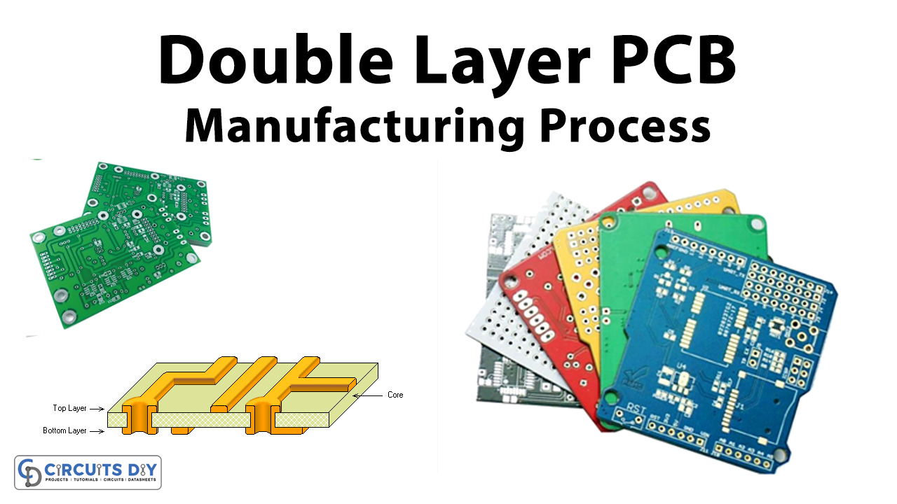
Introduction to Double-layer PCB
Double-layer PCB is very identical to a single-layer PCB. However, they have two sides that have copper conductive material. That allows the tracks to cross over each other. As a result, it gives higher density to circuits without a point to point soldering. But this type is more complex than a single layer PCB and that’s why used for complex circuits. The double-layer is the most popular type of PCB that has so many applications.
Construction of Double-layer PCB
The construction of a double layer is very similar to the single-layer PCB with some exceptions that is, the lamination is done on both sides of the board. The design is first created on software like ORCAD, PROTEL, etc. The layout is designed there. After designing, it gets printed on paper. After that, it gets ironed on the PCB Board. Moreover, it gets finished the etching process. After that, PCB gets ready for the components to be inserted. The step by step construction is given below:
Schematic
The first step is to construct the circuit design on the software. Once the design is made, it gets a recheck if there are any mistakes.
Thermal Transfer of layout
The substrate is created by ironing the design on the thin PCB board. Copper is already affixed to both sides of the layers of the board. And, then etched away to illustrate the design from printed films.
Inner Layer Printing
Now, the laminate panel is covered by a photosensitive film called the resist. This resistance is made from photoreactive chemicals. This chemical gets harder after exposure to ultraviolet light.
The resistance then passed through the ultraviolet light to get harder. This shows the pathways of copper. The excess photoresist gets removed by washing it with an alkaline solution.
The chemical identical to the alkaline solution is used to remove unwanted copper. And, the hardened photoresist remained unscathed.
Inspection
An optical punch device drills a pinto to keep the layers mobilized. After that, another machine inspects the board to make sure that there are no errors or flaws.
Lamination
The epoxy resin layer goes into the alignment compartment. Then a layer of substrate goes over this epoxy resin pursued by copper foil. Lastly, one more copper layer is applied. Copper foil is laminated on both sides
Drilling and Plating
To press the layer, the mechanical press is used. Then, PCB goes to laminating press which applies pressure and heat to the board. After that, holes are drilled into the layer, and the remaining copper gets removed
Now, the panel is plated with a copper layer and a thin tin guard is layered on the board. The thin tin guard is used to protect the copper.
Etching and a Solder Masking
The chemical that was used before removes the unwanted copper and creates the connection on board. Then the solder mask is applied. Solder mask fabricates on both sides of the board. Solder mask usually involves those green colors that can be seen on the PCB board. Unwanted solder mask gets removed from ultraviolet light.
Silk Screening and Testing
Silk screening prints the crucial information on both sides of the board. The board gets completed with a solderable finishing that increases the quality of the board.
Lastly, the designer then tested the PCB, whether it’s working or needs troubleshooting. This will complete the whole process of manufacturing single layer
Conclusion
In short, we explored that construction and manufacturing are almost the same steps that are described above. Double layers are more useful and effective for complex circuits