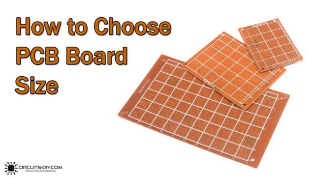
In Today’s day & age, Mastery in PCB design & fabrication is a mandatory skill for every Electrical & Electronic Engineer. At its core, A Printed Circuit Board (PCB) is a conductive plate on which you can align & place various elements that collectively constitute an electrical circuit. The domain of PCB designing is vast & complex. Beginners can easily get bewildered by the huge amount of terms & description. So, Today’s article will serve as a PCB terminology guide & will cover the most common terms & references used in PCB designing.
Throughout the course of studying PCB design & fabrication you will come across a number of terminologies that are quite frequently used in everyday design work & applications. Those common terms are as following:
JLCPCB is the foremost PCB prototype & manufacturing company in china, providing us with the best service we have ever experienced regarding (Quality, Price Service & Time).
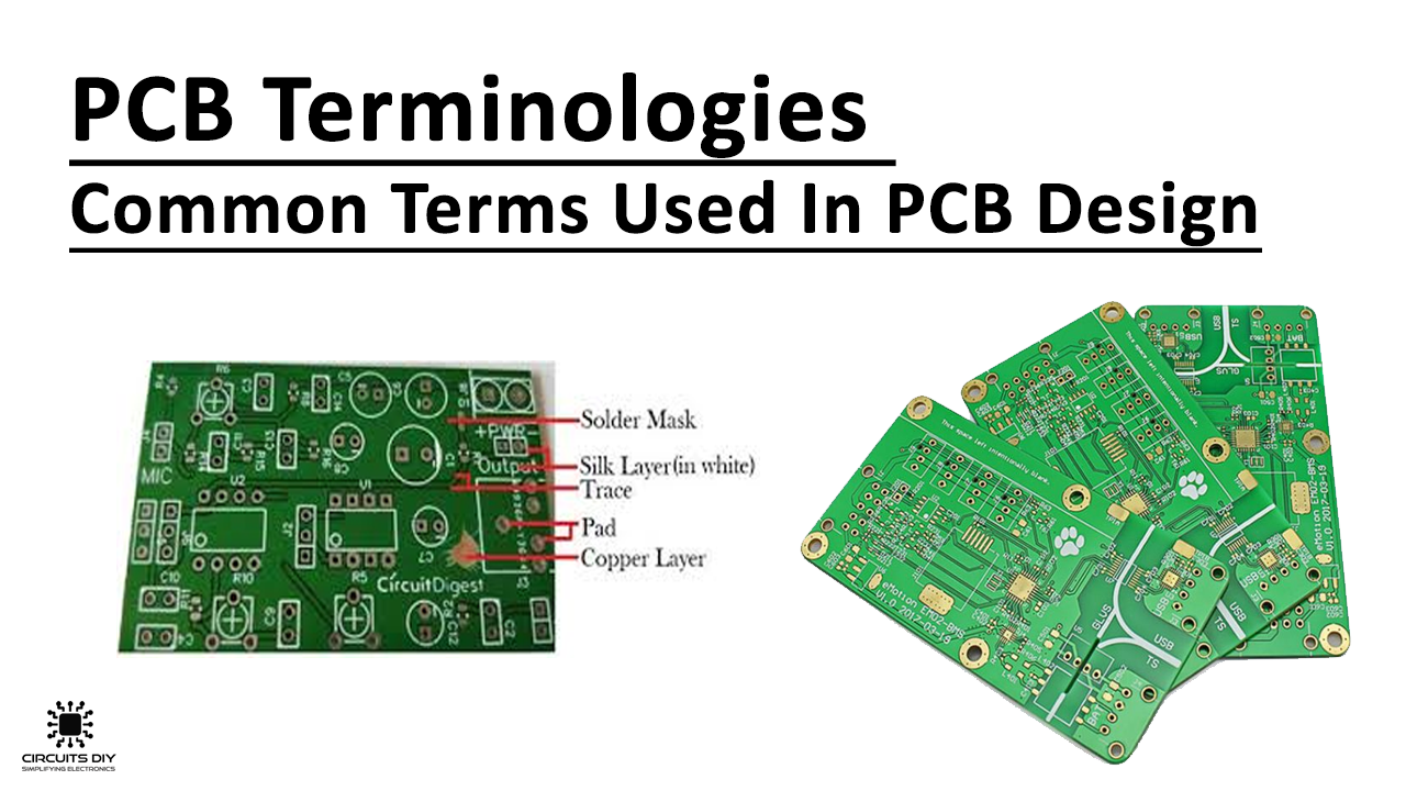
Common Terminology Used In PCB Design
1) Active Components
This term points to the kind of components that depend upon the directional flow of electrical current such as transistors, diodes, SCRs & ICs, etc.
2) Annular Ring
The area between the edge of the via and the copper pad with that hole is the annular ring. The extent/quality of the copper connection of any component on the PCB is directly proportional to the width of its annular ring.
3) Board
A word used to describe the central section of an electronic component. It does not include the component’s pins, leads or accessory parts.
4) BOM
BOM stands for Bill Of Materials. It allows you to generate a list of all the parts present on the PCB board. BOM allows you to calculate the approx cost of the PCB & also helps you to cross check the parts you might have mistakenly forgotten.
5) DRC
DRC is an acronym for design rule check. It runs a software verification of all the parts on the PCB, ensuring that there are no sources of errors such as small drill holes or traces placed too close together.
6) Footprint
Footprint is the collection of pads and outline which make an individual component.
7) Functional Test
A type of electrical test that provides the go or no-go on the finished PCB. It is a battery of electrical/electronic tests that judges the assembly & viability of the PCB by simulating it’s final electrical environment.
8) Gerber File
Gerber file is sent by the user to the manufacturer to make the PCB. It contains information about drill size, where to make holes, how tracks are connected, naming of components, etc.
9) Copper Traces
Copper Traces provide electrical conduction between pads and vias or between two pads and vias. Width of track varies according to the current flow through them.
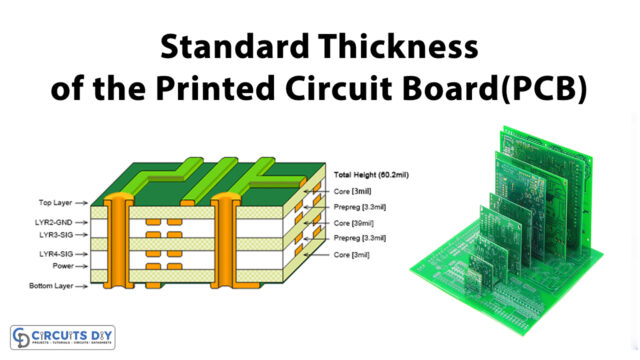
10) Layers
Everything which you draw is on layer. Each layer has different physical properties. For e.g. top layer is used to draw the component layout, the bottom layer, or inner layer are used for making connections between components and many more are also present.
11) Laminate
A PCB terminology referring to the combination of different materials through heating, adhesive, and welding methods to create a new PCB material with multiple layers.
12) Pad
A pad is a contact point for connecting components with a via through soldering.
13) Solder Mask
The solder mask is a layer of material, usually consisting of an epoxy resin, which isn’t compatible with the solder itself. This material covers the entire PCB, except those areas where content needs to be soldered.
14) Silkscreen
This is a layer of epoxy ink that covers the PCB containing component names & positions. The labels included on silkscreens helps to direct workers through the assembly process.
15) Via
Via allows the current to pass through the board. Vias have conductive copper interiors to maintain an electrical connection.
Blind Via:
Blind vias are through-holes that connect inner layers of a PCB, but they cannot be seen from the exterior of the PCB.
Buried Via:
Buries via is a via connecting the top layer to one or more inner layers. It can be seen from only one side of the PCB.