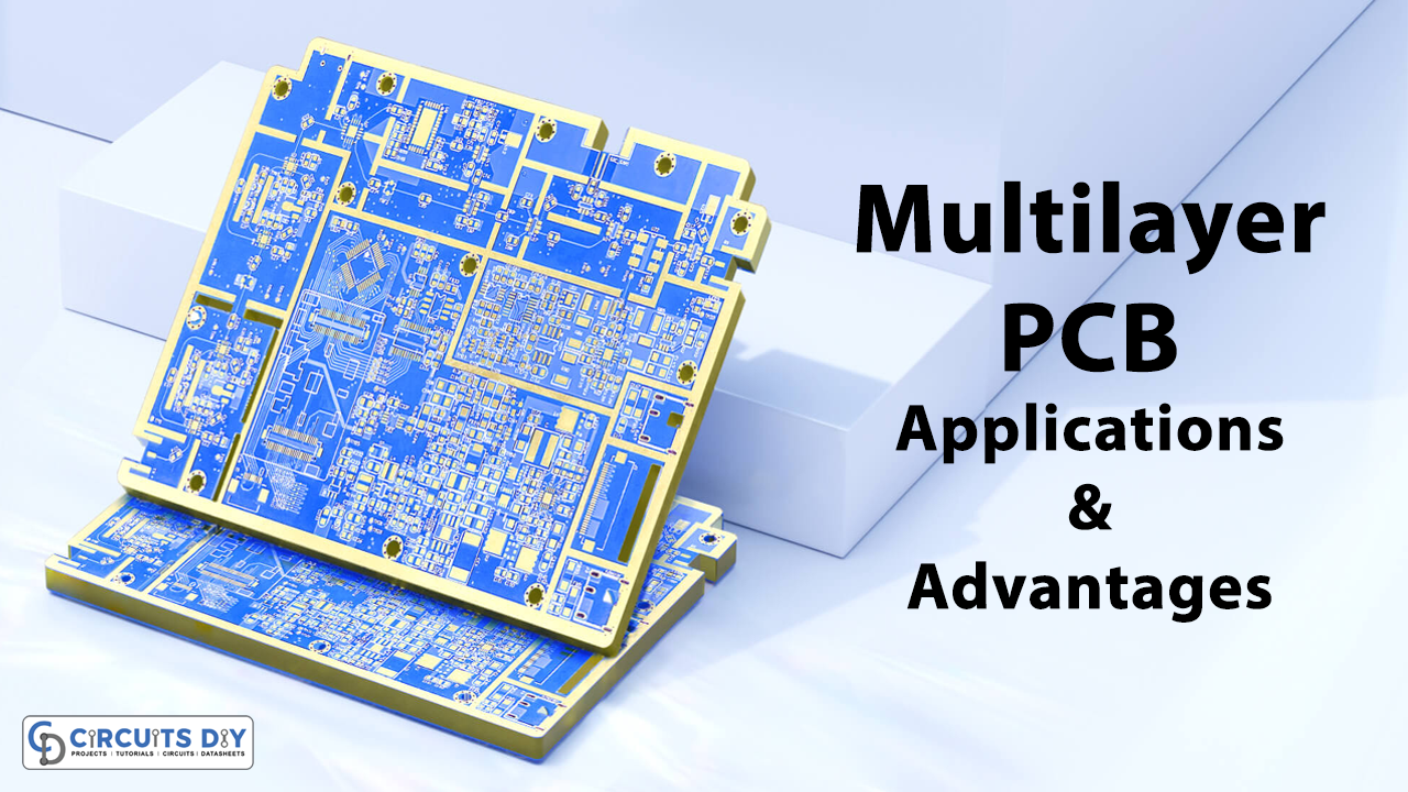
Introduction
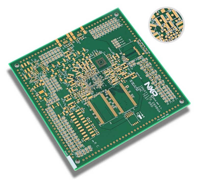
Printed circuit boards are the major part of electronic circuits. Every effective electronic device use printed circuit boards to make efficient circuitry. It proceeds with the design technique that converts an electronic layout that is designed by the circuit designer into a physical circuit board. However, there are three different ways to design the PCB, a single-sided PCB, a double-sided PCB, and a multi-layer PCB. Multi-layer PCB is the major and most beneficial type of Printed Circuit board. Multi-layer PCBs include three dual-size copper layers that enable a complete layer for the ground plane. We can operate thousands of components and ten thousand vias in multilayer PCB. Greatly used multilayers have less than 10 conducting layers and have a thickness of 1.5mm.
In this article, we are going to inquire into multi-layer PCB. In the other words, In other words, we will learn its applications and advantages.
JLCPCB is the foremost PCB prototype & manufacturing company in china, providing us with the best service we have ever experienced regarding (Quality, Price Service & Time).
Advantages of Multi-layer PCB
Multi-layer PCB has more benefits than other types of PCBs. These advantages include the below-mentioned facts
Light Weight :
The construction of multi-layer PCB is less in weight as compared to the other types of PCBs. Connectors get reduced or even eliminated for some circuits. As a result, simplify the construction. And, this empowers more mobility to the circuit. Therefore, more beneficial for electronic devices.
Small Size:
These PCBs certainly have a small size because of the design. As we all know that recent and modern electronic needs smaller sizes. The gadgets and electronic equipment are getting smaller day by day. So, the compact sizes of PCBs help in making smaller devices.
High Durability Rate:
Multi-layer PCBs easily withstand high pressure and thermal expansion. So, it increases the durability of circuits. Moreover, it uses multilayers for the insulation between the layers. Binding all layers with protective material. And, this also includes durability.
One Connection Point:
Rather than multiple connection points, it only has one connection point. Therefore it advantages the electronic components. Since most modern devices need tiny sizes.
Powerful:
Since they integrate multiple layers in a single printed board. That’s why they are a higher density of assembly which enables them to attain greater capacity.
High Speed:
The close-quarter enables the board to be more connective. As all the components are near to each other. Consequently, results in a higher speed.
Applications of Multi-layer PCB

- In Computer Electronics: Multilayer PCBs are highly used in computer electronics. Since computer needs high efficiency and speed. Therefore, they are highly preferable. And, that’s why used in the motherboard
- Medical Appliances: Multilayer PCB is considered promising for medical equipment. The reason is its functionality and durability. As we have discussed earlier that it has a high durability rate.
- Telecommunication: It has various applications in telecommunication. For example, they are used in GPS and satellites. Also, it has applications in signal transmission.
- Military: Highly preferable in military applications. As it has high speed and low weight. And, also it has high durability.
- Industrial Applications: Because of its above-mentioned specialties and advantages, it is highly used in industries and industrial pieces of equipment.
Related posts:
 Top 5 PCB Design Tools & CAD Softwares For Beginners
 What is Flex PCB? Advantages Disadvantages & Applications
 PCBA-Online: Top PCB Manufacturing And Assembly Service
 Importance of Monitoring PCB Temperature
 Double-layer PCB- Manufacturing Process
 SMT PCB Assembly Process - A Complete Guide For Beginners