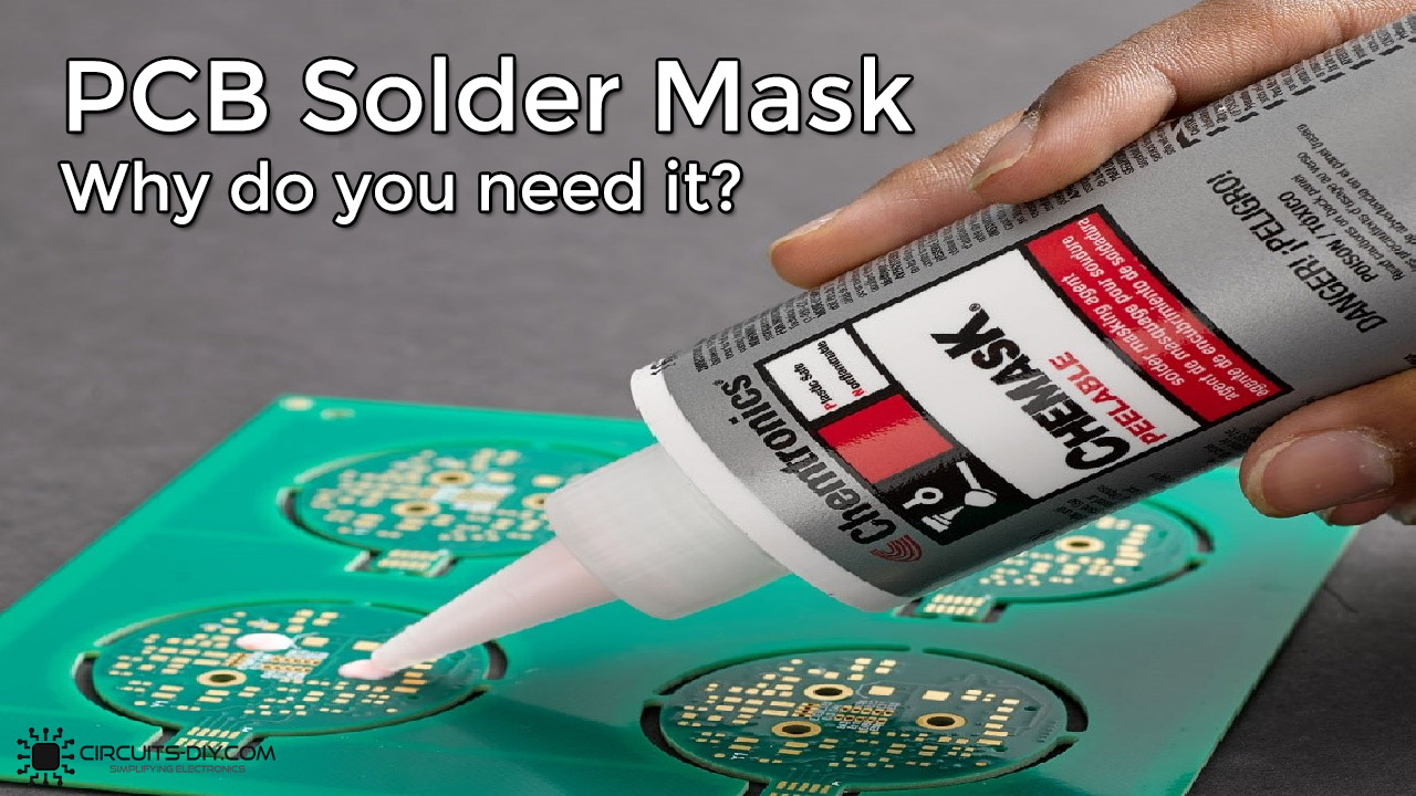
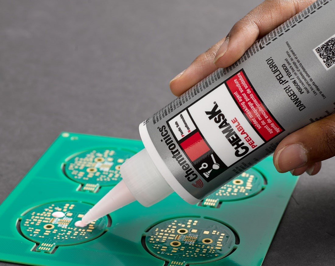
PCB Solder mask or PCB solder stop mask or solder resist is a thin lacquer-ish layer of polymer; it is applied to the copper traces of a PCB board for protection against oxidation and to prevent solder bridges; the formation of an undesirable electrical connection between two conductors by means of a small blob of solder. PCBs use solder masks to prevent this from happening. Solder mask does not only function to handle soldering assemblies; but, its presence is also essential for mass production assemblies that are soldered automatically using reflow or solder bath techniques. So, In today’s article, we will understand what is a PCB solder Mask, its types, and its need in PCB designing.

Types of PCB Solder Mask
There are 4 main types of PCB solder masks available in todays market which are mentioned down below.
- Top- and Bottom-side Masks
- Epoxy Liquid
- Liquid Ink Photoimageable
- Dry Film Photoimageable
Top- and Bottom – side Masks
A topside solder mask allows the PCB designer to identify the openings in the green solder mask layer; that are already added to the PCB by one of the epoxy, ink or film techniques. PCB parts can then be soldered onto the board using those identified places. The pattern of conductive traces on the topside of the circuit board is called top traces; while, the bottom side mask specifies openings on the lower surface.
Epoxy Liquid
Epoxy liquid is a lower cost type of solder mask. It is a quick setting thermosetting polymer. It utilizes Silkscreening printing technique that uses a woven mesh to support ink blocking stencils or patterns. The mesh creates open areas for ink transfer. After that, the final finishing process involves thermal curing.
Liquid Ink Photo-imageable Solder Mask
Liquid photo imageable solder mask comes as an ink formulation. The ink can be silkscreened or sprayed onto the PCB; the PCB is then exposed to the pattern and developed. Also, One type of process commonly used with liquid ink formulations is hot air surface leveling (HASL). It requires a clean environment, free of particles and contaminants. After that, that UV light exposure stage, the mask is removed using high pressure water sprays called developers.

Dry Film Photo-imageable Solder Mask
Dry film photo imageable solder mask works with PCB boards using vacuum lamination, then exposed and developed. After developing, openings are created in the pattern and parts can be soldered to the copper pads. After that, Copper is layered onto the board inside the holes and on the trace areas using electrochemical processing. Tin is applied to protect the copper circuitry. After that, The dry film is then removed and the exposed copper etched. Finishing also involves thermal curing.
Use of PCB Solder Mask
PCB solder masks become very useful in the mass assembly and production of PCBs. The solder mask protects the copper traces; so that, the solder bath allows the tinning of each copper pad on the PCB board in one application without allowing any solder to come into contact with sealed areas.