
Introduction
Every other device around like smartphones, computers, cars, robots, etc is integrated with the printed circuit boards. To make these electronic products more reliable from the exposed mechanical and thermal effect, strain rate measurement on a Printed Circuit Board(PCB) is necessary. During the manufacturing bending strain may occur while installation of power rails, connectors, terminals, batteries, etc. Similarly, breakage can happen while mounting the components. Also, stress cracks, transient strain peaks, and elevated mechanical stress can happen. During the transport operation, mechanical load and vibration can also cause malfunction. In the same vein, the thermal effect can cause cracks. Hence, these all factors can damage the printed circuit board and so the electronic devices. Therefore, measurement of strain is highly preferable.
How to Measure strain on PCB
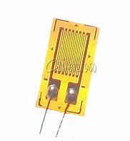
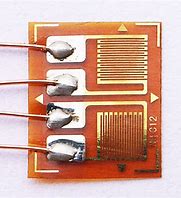
Expensive methods like X-rays, and CTs are not sufficiently encouraging. And, numerical methods are very limited because they are based on a mathematical approach. Therefore, physical analyses and measurements are needed for the strain measurement. But, the strain values are only reliable to measure the deformation of the PCB. Therefore, strain gauges are available in the market to estimate the accurate deformation. The only challenge is to install these strain gauges on the PCBs that usually have small sizes. However, there are gauges in the market that can easily be mounted on the printed circuit board.
Where to Measure Strain on PCB
It is not possible to check every section of the Printed circuit board. It may require a lot of time and money. Thus, the measurement of the strain can be achieved in the areas where there is a high risk of breakage and exposure. For example, the corners of the PCB are critical mechanically. In the same way, stuff regions that have bigger elements can increase stiffness. Similarly, the areas which are close to interconnect. These regions are meant to be measured.
Maximum Allowed Strain
Generally, the designer and the manufacturer agree on the values. But, some manufacturers also specify the value limits. But, for the measurement equipment, a sampling resolution of 12 to 16 bits is favored and the low pass filter is suggested. Also, a minimum of 50 Hz frequency is allowed. Moreover, a frequency of 2KhHz is recommended.
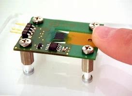
Installation of Strain gauge on PCB
The surface of installation should have great adhesion between the strain gauge and the Printed circuit Board. For this purpose, the upper layer gets removed by a face milling cutter. After that, the surface gets roughed by using sandpaper. Further, the adhesive surface gets cleaned. Finally, the bonding of the strain gauge can be performed using any fast adhesive material.
Conclusion
The strain rate determines the lifespan of the printed circuit board. Hence,e strain rate measurement on PCB is the essential part of the process. The strain rate is influenced by the maximum principal strain. Moreover, it is also affected by the changing of the impulse. Thus, strain gauges are designed to estimate the deformation of the printed circuit board with a high accuracy rate so that it makes the electronic device reliable and more durable.
Related posts:
 All about Surface Mount Technology (SMT) of PCB
 History of PCB Board and Evaluation
 PCB Cleaning Solutions 101 | Ultimate Guide To Keep Your PCB Clean
 Simple Digital Voltmeter Circuit with PCB using ICL7107
 Printed Circuit Board Arrays | A Complete Guide For Beginners
 Common PCB Design Pitfalls To Avoid While Ordering Online


