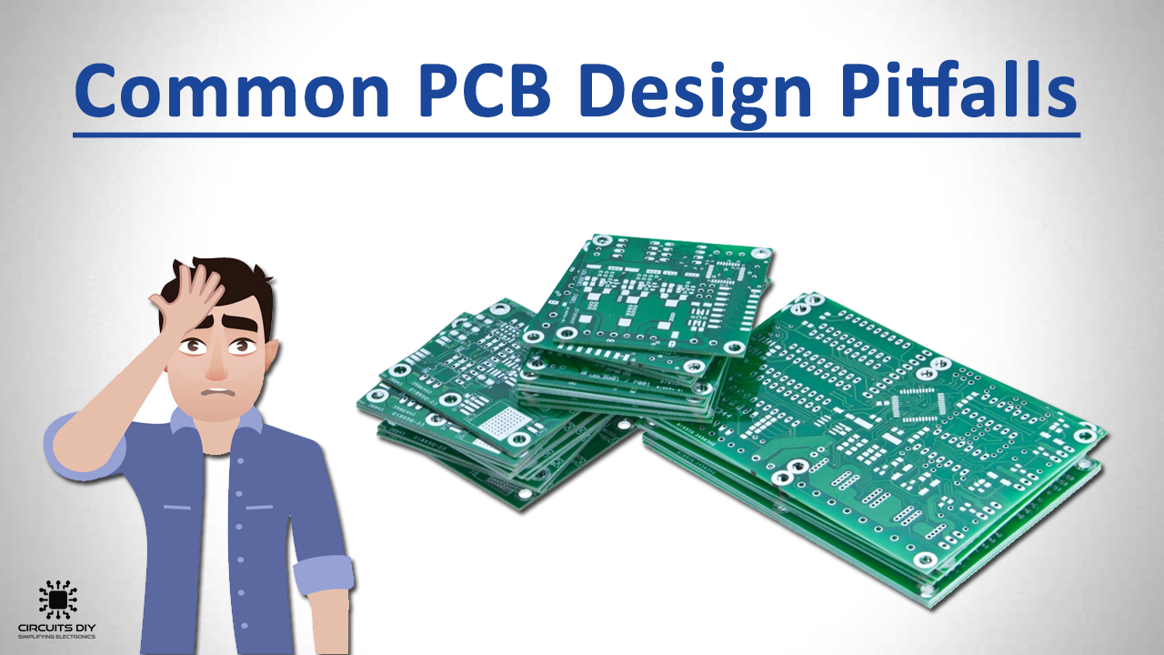
You have finished your design & have generated your layout, Gerber, BOM & pick and place (X – Y) files. you submit it to the PCB manufacturer expecting a small bill with fast delivery time. But what’s that?!!, the manufacturer has replied you back with an email, pointing out a heaping list of design errors, which in turn costs you more time & money. Design errors while ordering PCBs are a common occurrence of which even the most novice engineers are not above. In today’s article, we are going to go over the Top 6 most Common PCB Design Pitfalls you can face while ordering PCBs online.
PCB designing is an intricate process with a lot of variables & it is understandable for beginners to end up making a mistake in the initial designs, but which in turn, also hurts the PCB production timeline & cost. The following are some common PCB Design Pitfalls you can avoid when ordering your next PCB.
Common PCB Design Pitfalls
1) Not Leaving Enough Edge Clearance
A general mistake beginners do is not leaving enough edge clearance. Since a PCB is plated with copper and then covered with a layer of protective material. During the manufacturing process, the edges of the board can get cut off including the protective coating, which in turn exposes the copper. As a result, your circuit might corrode over time or even be prone to a short circuit. Make sure to leave an adequate amount of edge clearance before turning in your circuit to the manufacturer.
2) Overcomplicating Your Design
Avoid placing SMT/Through-hole components on both sides of the PCB unless absolutely necessary. This makes the design more difficult to comprehend for the manufacturer & will actually cost you more as your board will have to go through various cycles of the pick and place machine.
3) Incomplete Pick & Place (X – Y) Files
Pick & Place files or (X – Y) files contain the basic information as to where the machine must place the respective parts. You have to send this file to your PCB manufacturer with your layout designs. Be sure to verify all this data and check whether you’ve sent all the information. Following is a list of information that should constitute your pick & place file.
- Component Reference Designator
- Part Number
- Part Description
- Manufacturer Part Number
- Mid-Point X(mm)
- Mid-Point Y(mm)
- Orientation Angle
- PCB Layer Side
4) Placing Silkscreen on Pads
Placing silkscreen on your pads makes the soldering process difficult for the manufacturer, which may also lead to design discrepancies on the manufacturer’s end. Always keep an adequate distance of at least 0.003” between the silkscreen & the solder mask.
5) Incorrect Size or Shape of Component Footprint
Check whether the components you are using in your PCB design will actually fit the pads you have designed on the PCB. Mention all these components in your BOM. Make sure whether all parts will fit the board correctly or will be too cramped or close to the edge. If the part footprint size is wrong, there’s a good chance it won’t solder properly and may even break.
6) Using Multiple Drill Bit Sizes
Another mistake that may end up wasting your money is using multiple drill tool sizes. Simply make all your holes and Vias the same size instead of different sizes.
So, by avoiding the above PCB Design Pitfalls, you can save both time & money on your PCB designs & ensure a productive experience for the manufacturer.