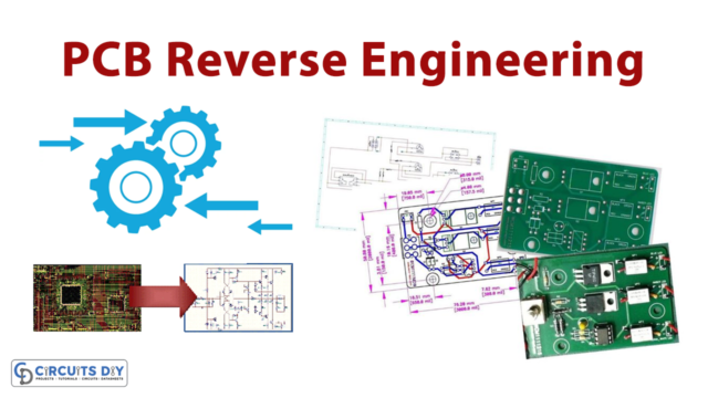
PCB Layout Designing is an essential skill that every electronics enthusiast must-have. Whether he be a student, an industry professional or a hobbyist. Proper PCB Layout design is an integral part of any PCB manufacturing process. Without proper care, Poor PCB layout designing can lead to function and reliability problems. So, in this project, we are going to reveal the top 7 PCB Layout Design Tips & Best Practices For complete Beginners.
PCB layout designing is a skill requiring knowledge of not only PCB CAD systems but also of a variety of quality standards and design rubrics to ensure that the basic circuit design is successfully imprinted to an overall PCB that can be manufactured in an electronics circuit manufacturing environment. In order to be flawless in Layout design, design engineers use a number of techniques. Out of those many, Following are the Top 7 PCB Layout Design techniques & tips, which you can use to take your PCB layout designing skills to the next level.
I have used PCBWay many times now, and I have never had any complaints. I use PCBWay both professional and for personal projects, and I have ordered more than 30 different PCBs. If any error with the uploaded data, I quickly receive a response with the issue.

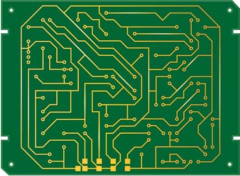
1) Focus on Sizing of Traces
We most commonly use length, thickness, and width to control the resistance of a PCB trace. You can’t really change the physical properties of copper, so focus on the trace size, which you can control. Use a PCB trace width calculator to determine how thick and wide your traces should be for your application. Aim for a 5°C temperature rise. If you have extra space on the board, use bigger traces, as they don’t cost anything.

2) Leave Room Between Copper Traces
Leave a proper amount of space between copper traces and fills to prevent shock hazards. Solder mark isn’t always a reliable conductor, so make sure there is a good amount of distance between the two.
For cheap PCB Prototypes under 5$ please visit: www.pcbway.com
3) Make Small Loops
High-frequency loops should be made as small as possible. Smaller the loops, the lower will be the inductance and resistance Placing loops over a ground plane further reduces inductance. Having small loops reduces high-frequency voltage spikes. Small loops also help to reduce the number of signals that are inductively coupled into the node from external sources.

4) Keep Analog Traces Separate From Digital & Noisy Traces
Keep high frequency and noisy traces away from traces that you don’t want noise on. Because, placing parallel traces close together can capacitively couple the signal together, especially if the signals are of high frequencies.
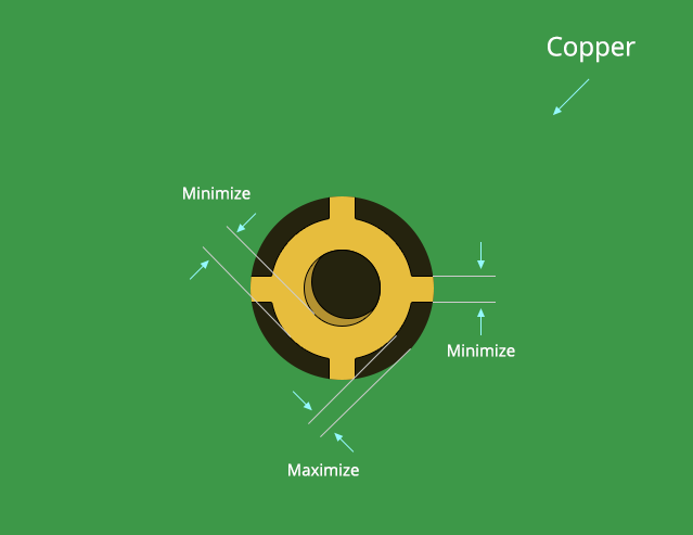
5) Thermal Relief
Provide proper thermal relief by making connections between a trace or fill and a component pin small enough in order to make the soldering easier. If there is no thermal relief on component pins, then the component may be a little cooler because there’s a better thermal connection to traces or fills that can dissipate heat, but it’ll be harder to solder and de-solder.
6) Layout Ground Is Not The Ground
By the rule of thumb, the layout ground is not an ideal conductor. Take care to route any noisy grounds away from signals that need to be quiet. Design ground traces big enough to carry the currents that will flow. Making ground plane directly under signal traces lowers the impedance of the traces.
7) Always Make the Final Manufacturing Output Files
Once the final layout is complete and you are ready to move on to the PCB assembly phase. Be sure to properly document all information about component sourcing, generating assembly drawings and Gerber files. Remember that you are building a circuit board and the board will only be as successful as the manufacturing documentation that you create.
So, By following the above Top 7 PCB layout Best practices you can improve your PCB layout designing skills