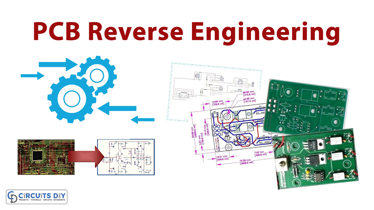
Engineering is a tremendously diverse field that constantly innovates. Engineers invent products that have never been seen. The true challenge is how we can create such a fast-paced era. But there is a solution. Yes! Reverse engineering. When it comes to igniting creative and productive brains, Reverse Engineering (RE) plays a significant role.
The PCB reverse engineering process involves disassembling worn-out items to analyze how individual components function before merging prior inventions into new products.
In short, Engineers and technical professionals do not need to build the PCB from the beginning or scratch in reverse engineering. Instead, they employ various tools and approaches to extract information about the Printed circuit board and its architecture.
The benefits of reverse engineering for electronics projects
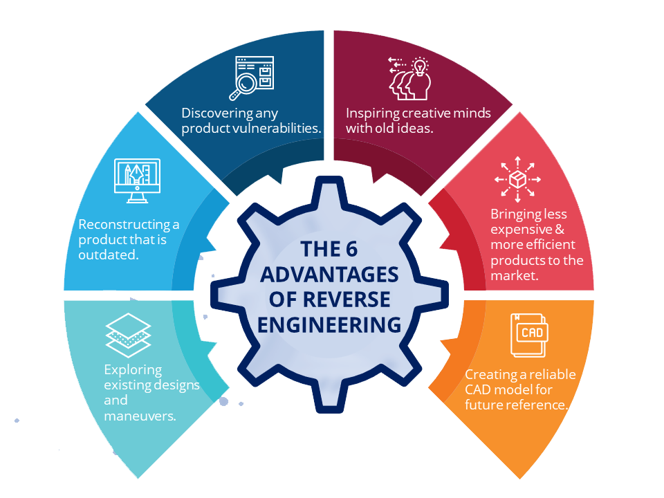
Reverse engineering can advance engineering in many ways, including by investigating current designs, recreating out-of-date items, and creating less expensive things. For instance:
- Reverse engineering makes it easier to redesign PCBs. In the case of legacy systems, this is extremely helpful.
- It helps us to remove obsolete semiconductors from old PCBs that are now out of compliance with environmental standards.
- Utilizing previously examined components during an upgrade saves time and money.
- The component’s functionality also increases with the new PCB design and related software.
- Reverse engineering allows you to build cost-effective designs, decrease waste from damaged and discarded boards, and restore and replace worn-out electronic circuits.
- Last but not least, reverse engineering opens the door to creative design. Engineers may link projects with prior knowledge and generate fresh ideas using reverse engineering.
How to choose a reverse engineering company
Knowing more about the company’s history is the best way to choose the reverse engineering service provider. Also:
- Look at the company’s ratings. If the reviews are favorable, move on to the consideration stage.
- Another factor is the caliber of the workforce; the organization must have resources in CAD, 3D scanning, and other relevant fields in addition to reverse engineering.
- Check their response time and whether or not they provide mobile scanning services.
How to reverse Engineer a project

When performing PCB reverse engineering, several processes are taken. These actions comprise;
- Collecting and analyzing data
- Drawing and scanning
- Adding the image to the appropriate software.
- Building a 3D PCB layout
- Developing schematics
- Create Gerber files
- Testing
Collecting and Analyzing Data
Data is crucial to every project, just like any other project. The PCB is wholly designed using this information. The information contains the following:
- Detailed PCB information is necessary for reverse engineering.
- Details on the components used on the PCB
- The specifications of each of these components
- The details of how each circuit functions.
- The data also contains any details that need to be created into a schematic.
Drawing and Scanning
Because a PCB already exists, It will assist you in designing your PCB. The PCB is therefore drawn on a piece of paper to begin the process. Using an image editor, it is first digitalized after being scanned with a scanner. The photos are then saved in a file comprised of layers.
Adding the Image To the Software
You may now submit the PCB image you have drawn and photographed and upload it t the website. This will aid you in the creation of your PCB design. However, you must provide the PCB picture in the proper format, such as PDF, DXF, or SVG.
Create a PCB Layout
You will now create the 3D PCB layout using your picture. You may make the PCB with the aid of 3D PCB designing software. You will design and test your PCB at this phase. Schematic, netlist, and layout are only a few of the features the software will include. The components that go on your PCB are up to you to choose. Even printing out the circuit diagram on paper is possible using the software. Furthermore, you save the design as an image file and print it from a printer.
Building a Schematic
A schematic is a circuit diagram used in PCB design to demonstrate how all the components on your PCB are connected. We must develop the schematic to outline what must be done and when. For instance, you must build a schematic for a project if you want to design a custom PCB.
Create Gerber Files
Your order includes Gerber files, which are utilized in manufacturing your PCB, besides using them as documentation of your board design. In this phase, we must create two files: a BOM file and a Gerber file.
Testing!
After creating the Gerber files, you must check the PCB for any flaws or problems. To test your board, utilize one of the several PCB designing software available. In addition to evaluating the board, you should look for any manufacturing mistakes that could have compromised the functionality of your design. A test can show, for instance, that you designed a defective component or an error in routing the traces on your PCB.