PCB designing is a complex and intricate process. Getting a PCB professionally designed by a PCB contract manufacturer; You, realize very soon how important it is to be on the same page as the design manufacturer; in order to get the PCB design to align exactly with your design needs without having to suffer through unnecessary quote delays. This leads us to realize that, having a basic understanding of common PCB terminologies can make co-operation with a PCB manufacturing company much faster and easier. In today’s article, we are going to go over an in depth PCB Glossary; In which, we are going to cover the most commonly utilized PCB design terms in PCB manufacturing.

PCBWay commits to meeting the needs of its customers from different industries in terms of quality, delivery, cost-effectiveness, and any other demanding requests. As one of the most experienced PCB manufacturers in China. They pride themselves to be your best business partners as well as good friends in every aspect of your PCB needs.
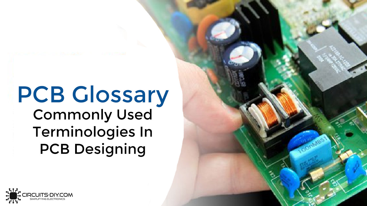
Glossary of Common PCB Terminologies
Following list represents the glossary of PCB Designing:
1) AOI
AOI stands for Automated Optical Inspection. AOI is a type of pre/post reflow soldering inspection that helps in detecting the quality of the soldering, common issues in soldering & component alignment before and after soldering. In AOI testing, a camera autonomously scans the device under test for both catastrophic failure and quality defects.

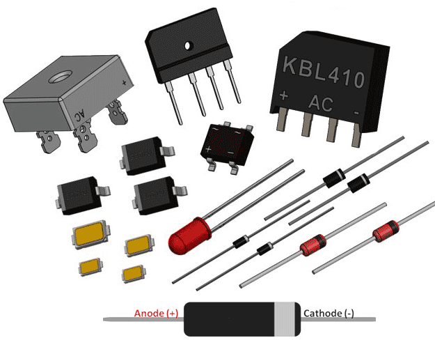
2) Active Components
This term points to the kind of components that depend upon the directional flow of electrical current such as transistors, diodes, SCRs & ICs, etc.
3) AQL
AQL stands for acceptance quality limit. It refers to the acceptable limit of faulty boards produced during a single production cycle. AQL is an important figure for monitoring the quality of an assembler’s production practices.
4) Assembly Drawing
An assembly drawing depicts the assembly requirements of a PCB. It includes the placement of components as well as the construction technologies. It also shows the methods and parameters needed to make it happen.
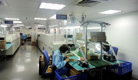
5) Assembly House
Assembly house usually refers to the manufacturing site, where all the assembly operation take place. These fab houses contain important PCBA equipment such as printer, mounter, reflow oven, and more.
6) Buried Via
A Buried Via is a type of via technology that connects the top layer of a PCB to one or more inner layers. A buried via can only be seen from one side of the board when looking at it from the outside.

7) Blind Via
Blind vias are through-holes that connect inner layers of a PCB, but they cannot be seen from the exterior of the PCB.

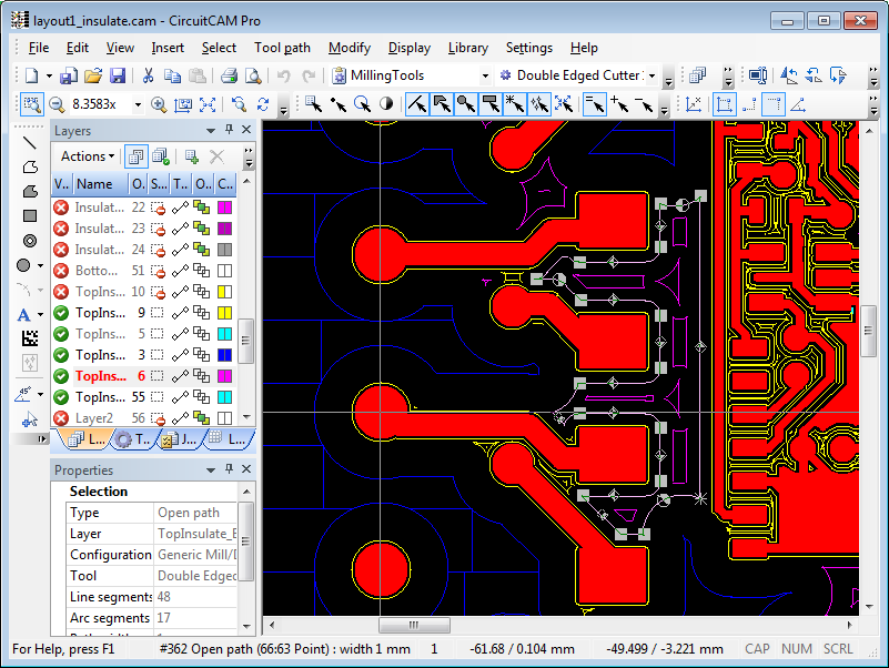
8) CAD
CAD stands for Computer Aided Design. CAD refers to those design software and tools that PCB designers use to design and implement the initial layout of a PCB board. These software also help in visualizing the PCB layout in a 2D/3D environment.

9) CAM Files
CAM stands for computer aided manufacturing. The CAM files contain all the physical information of a PCB layout translated into machine code and are essential for the fabrication of a PCB board. CAM files include the Gerber file for photoplotters and the CNC drill file.
10) DRC
DRC is an acronym for design rule check. DRC check is an essential evaluating step necessary for each and every PCB layout. It runs a software verification of all the parts on the PCB, ensuring that there are no sources of errors such as small drill holes or traces placed too close together.

11) DIP
DIP stands for dual in line package. It is a packaging technology; that is commonly used for THT components. DIP packages generally function as housing for integrated circuits (ICs).

12) Drill Hits
A term that refers to where holes will be drilled in a PCB design.

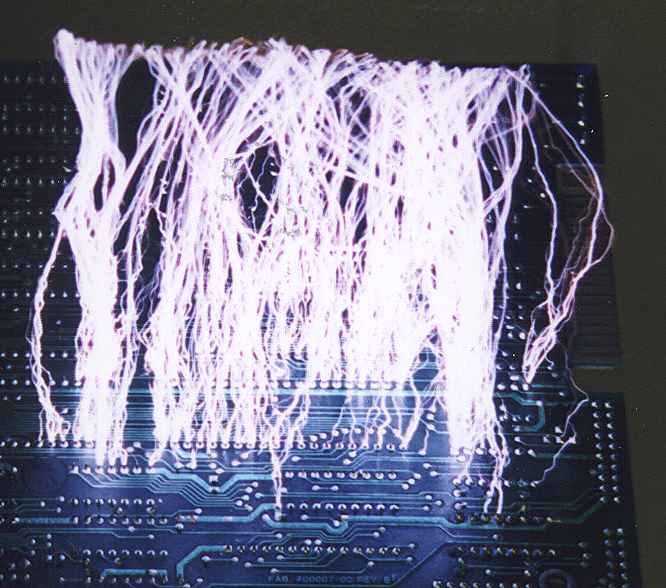
13) ESD
ESD is an acronym for Electrostatic discharge. ESD discharges are particularly harmful for PCB, causing them to short and burn out.
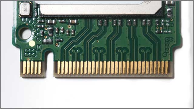
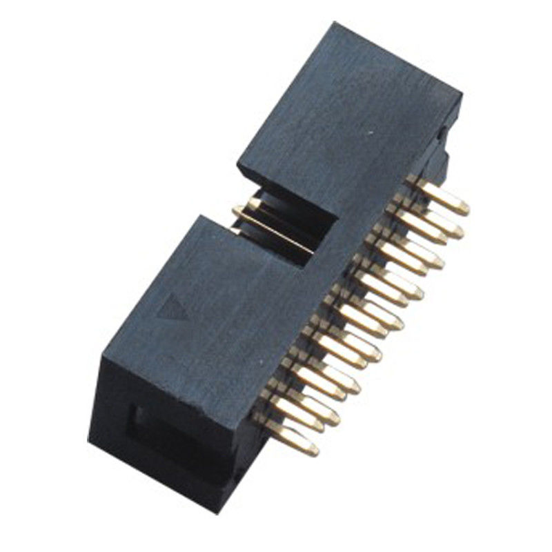
14) Edge Connectors
Edge connectors are a category of on board PCB connectors; they are designed to be installed in the edge of your PCB board, in order to facilitate an add- on card such as a GPU card.
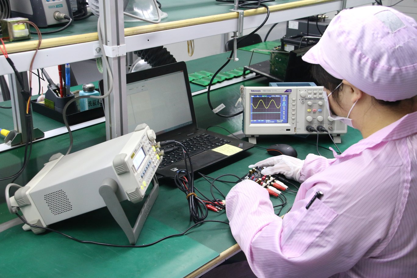
15) Functional Test
A type of electrical test that determines the fail/pass status of a finished PCB. It is a barrage of electrical/electronic tests that judges the assembly & viability of the PCB by simulating it in its final electrical environment.
16) Gerber File
Gerber file is sent by the user to the manufacturer to make the PCB. It contains information about drill size, where to make holes, how the tracks/routes connect, the naming of the components, etc.

17) Bill Of Materials (BoM)
Bill of material or BOM contains a list of all the necessary active and passive components that will go on the PCB. BoM also contains the electrical value of the components; As well as, the mechanical dimensions of all the components on the PCB.

18) FR4
FR4 is a material rating for any flame retardant material. It is also the most common material type used in PCB fabrication. The name also specifies that the resin material is capable of automatically extinguishing when it is aflame.
19) Laminate
A PCB terminology referring to the combination of different materials through heating, adhesive, and welding methods to create a new PCB material with multiple layers.

20) NC Drilling/Routing Machine
NC stands for numerical control. CNC (computerized numerical control) machines are an integral part of every PCB fab house that the designers use to drill holes and route traces on the PCB board.

21) Pad
A pad is a contact point for connecting components with a via through soldering.

22) Pick And Place Machine
A pick and place machine is a highly sophisticated PCB assembly machine; that serves the purpose of picking up SMT/THT PCB parts and places them in their area of designation on the PCB board.

23) Pitch
Pitch is the distance between two consecutive leads of a THT or SMT PCB part.
24) Route
A route or track represents an individual wire on a PCB board. A PCB route connects each individual PCB component with each other.
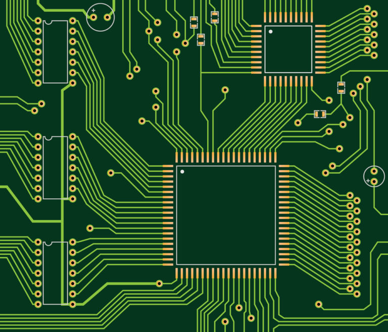
25) Silkscreen
This is the top most layer on the PCB board; The silkscreen is made out of an epoxy ink and contains the names of all the components on the PCB board. Typically, the color white is the most preferred for silkscreens as it is easier to see.
26) SMD
Short for surface mount devices, it refers to components designed to be soldered on the surface of PCBs, rather than through a thru-hole.

In conclusion, the above lists represent the PCB glossary of the most common PCB terminologies. By following the above PCB glossary you will be able to understand the basic terminologies used in PCB designing.
Related posts:
 How to Design a Printed Circuit Board - Voice Modulator Circuit
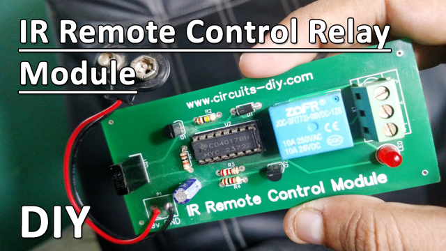 Infrared (IR) Remote Control Relay Module using TSOP1738 & CD4017
 All about Printed Circuit Boards(PCB) Inks
 Benefits of SMT Technology
 SMT Solder Paste Printing Process | Key Monitoring Parameters
 Factors that Damage Printed Circuit Board (PCB)