PCBs or printed circuit boards serve as the backbone of any design industry, allowing you to connect passive components, active components, and embedded devices together, into a specific form to fit the design need. A number of stages are involved in proper PCB fabrications which include designing, layout, routing, etching & troubleshooting. Being an intricate process, it is understandable why most newbies feel bewildered while dealing with a plethora of design tool options to choose from. So, in this tutorial, we will go through a step by step procedure on How To Design A PCB Using the EasyEDA Online PCB design tool. This tutorial will serve as a guide for beginners to PCB designing, but we also invite people who are experienced with PCB designing to brush up on their skills.
EasyEDA
Easy EDA is a free, no install, Web, and cloud based EDA CAD suite, featuring powerful schematic capture, mixed-mode circuit simulation, and PCB layout in a user friendly cross-platform browser setting, for engineers, educators, students, and hobbyists. It’s compatible with windows, mac, Linux as long as there is one browser on the OS and connecting to the network. You can draw schematics quickly using the available libraries on the browser. It offers Simple, Easier, Friendly, and Powerful general drawing capabilities along with Real-time Team Cooperation & Integrated PCB Fabrication services with the collaboration of JLCPCB.
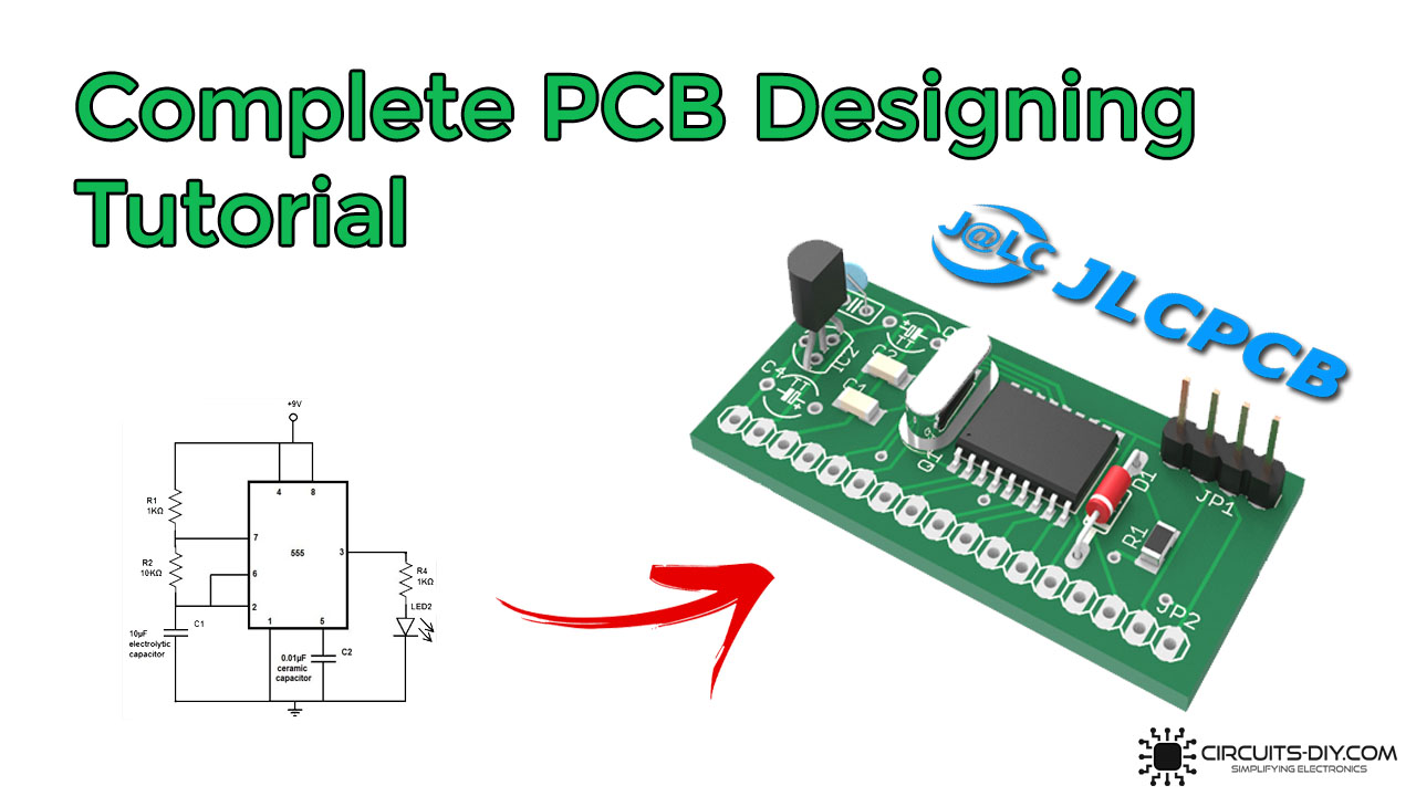
Complete PCB Designing Tutorial Using EasyEDA
Login/Signup To EasyEDA
1) Open your web browser (Google Chrome/Firefox). After that, type ‘EasyEDA’ in the search bar & press enter.
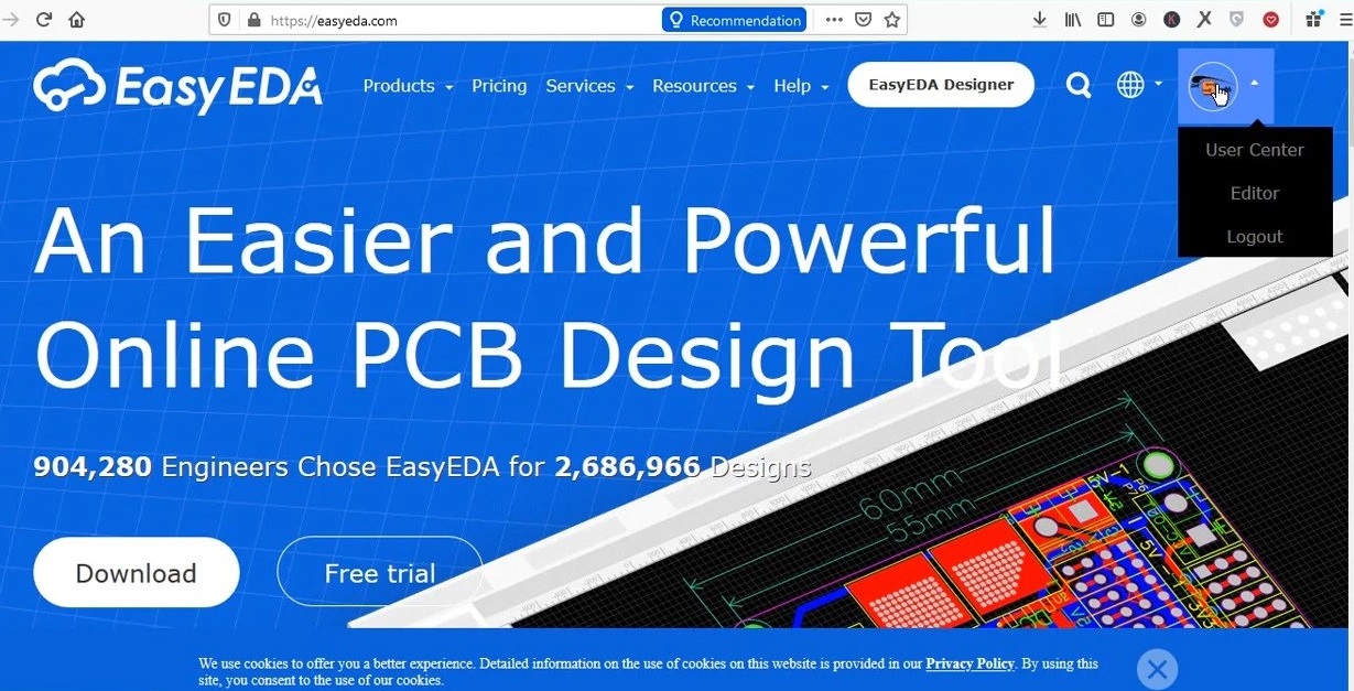
2) Register & login to your EasyEDA User account.
PCB Design Sample
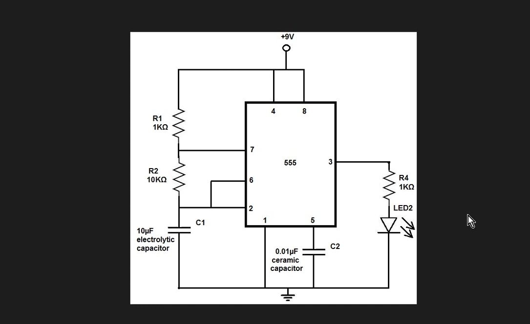
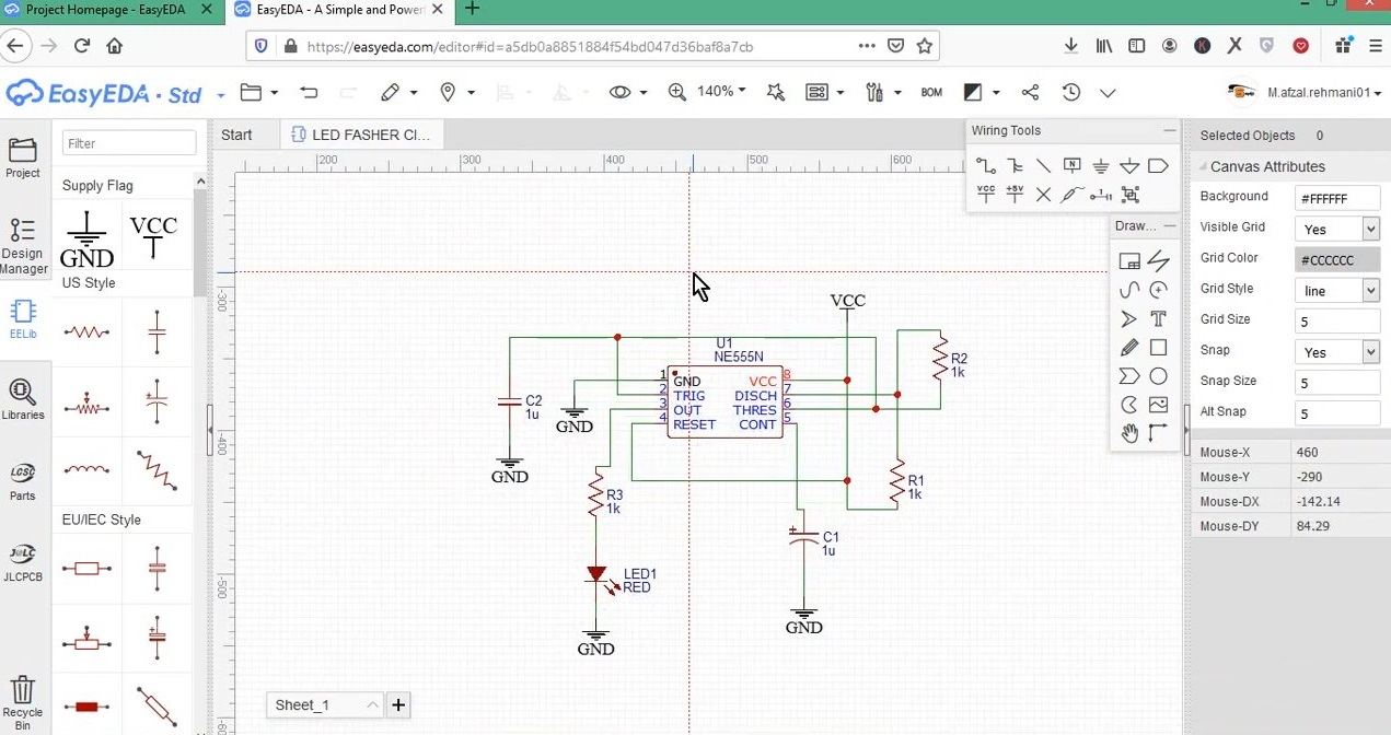
1) For the sake of simplicity for this tutorial, we will be designing a PCB layout for a simple LED Flasher circuit using 555 timer.
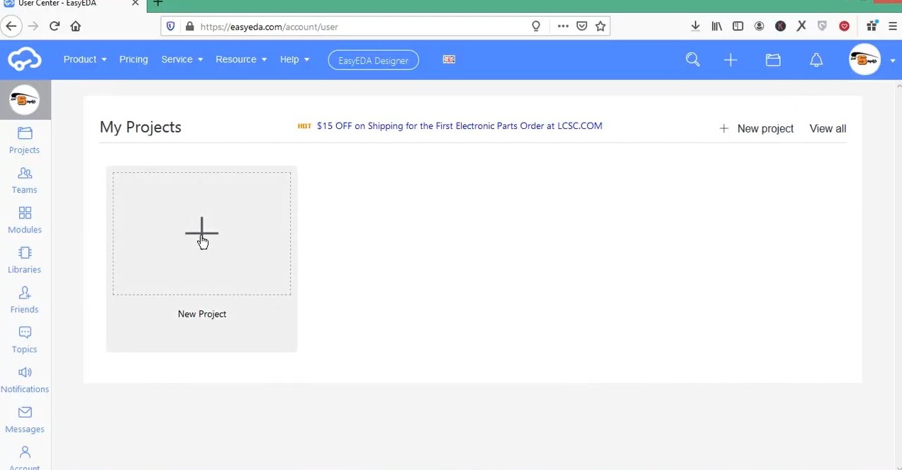
2) After logging in, click on New Project.
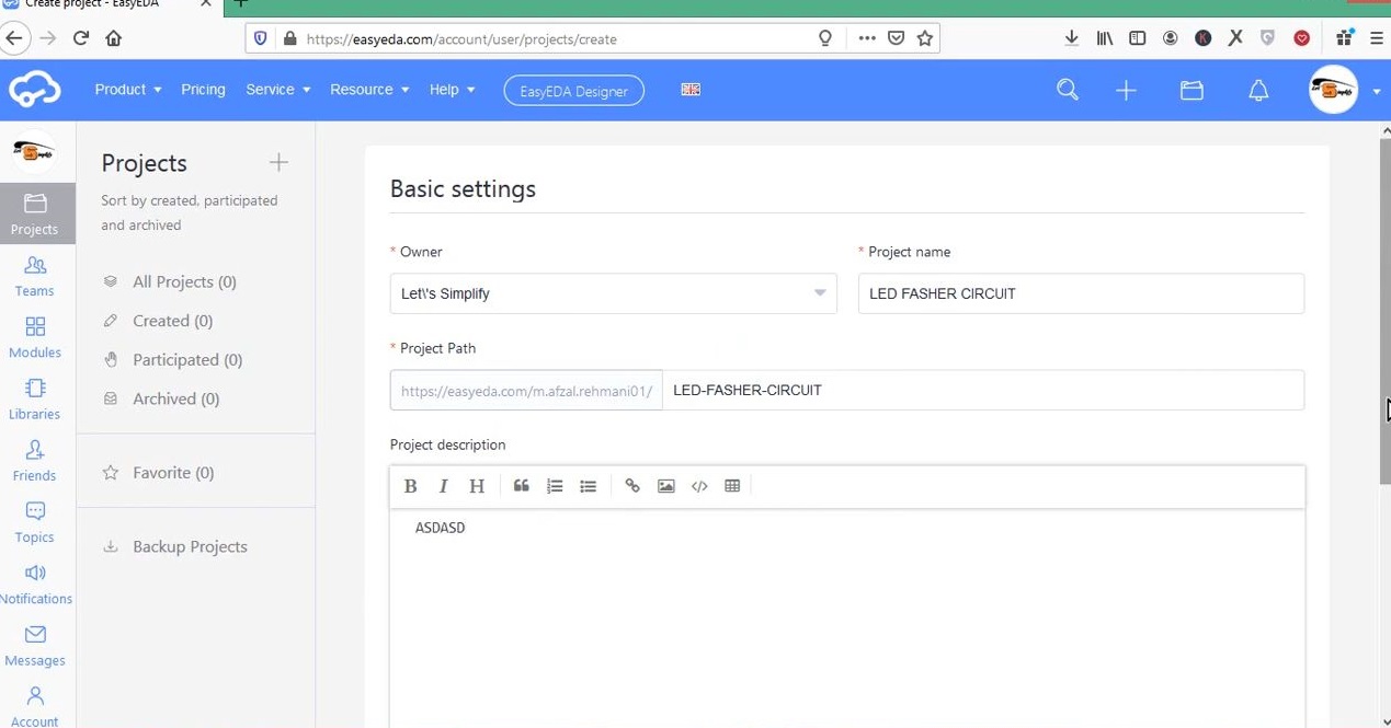
3) After that, Set the project name & description. After that, click on ‘Create Project’
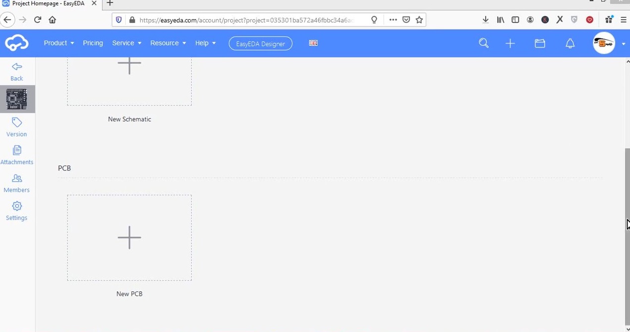
4) After creating the project file, you have the option to either start your design layout by drawing a ground up schematic or by directly plotting the PCB layout, choose the new schematic option.
5) After choosing new schematic, your will be directed to EasyEDA schematic design interface.
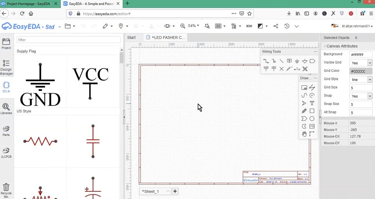
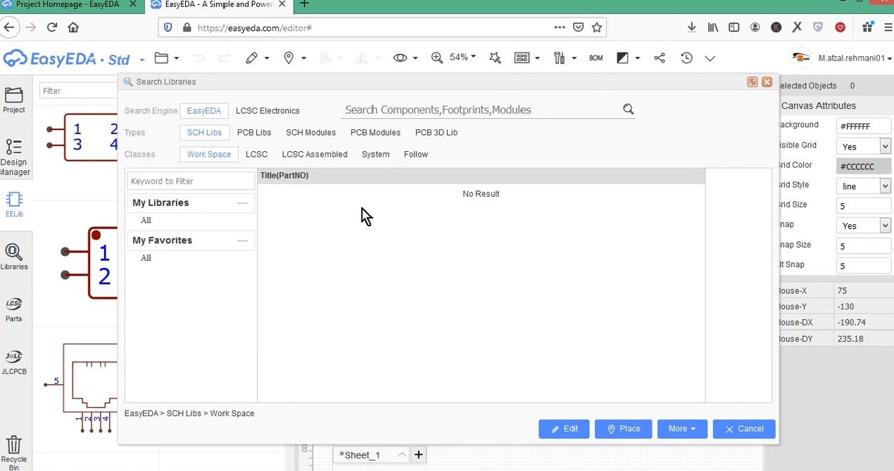
6) You can use the component panel on the left-side of the screen or the libraries option to search for your desired component.
7) Now draw the above circuit diagram in the workspace by selecting parts from the component list.
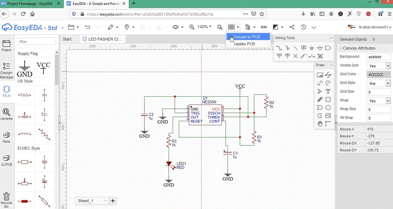
8) After completing the circuit, select ‘Convert to PCB’ option from the drop down menu in the toolbar.
PCB Design & Layouting
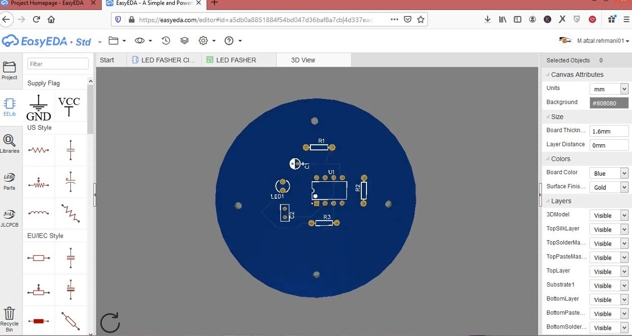
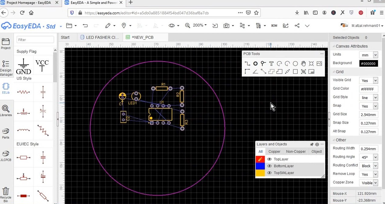
1) You’ll see the PCB Layout screen with your circuit into a rough PCB layout outside a rectangular board outline, here select ‘mm’ in the units menu.
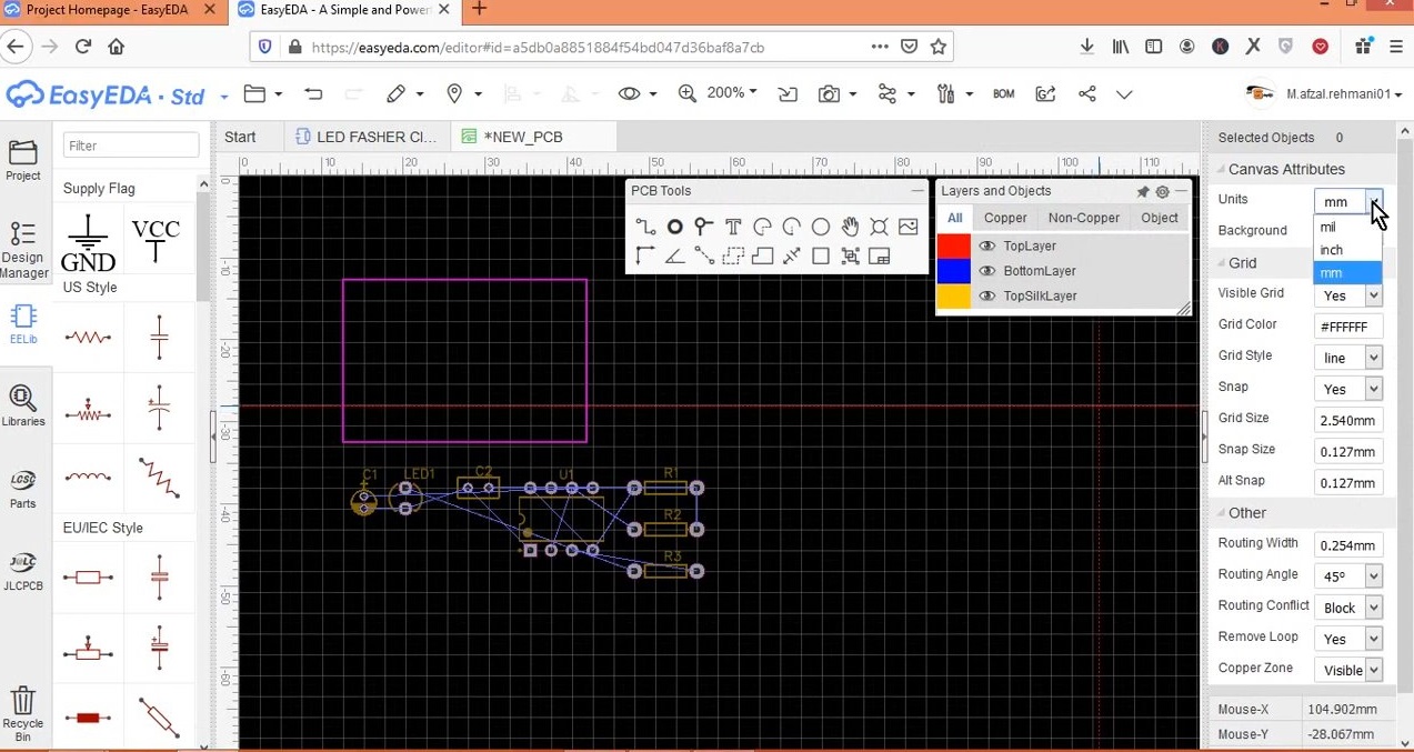
2) After that, Set board outline to ‘circular’
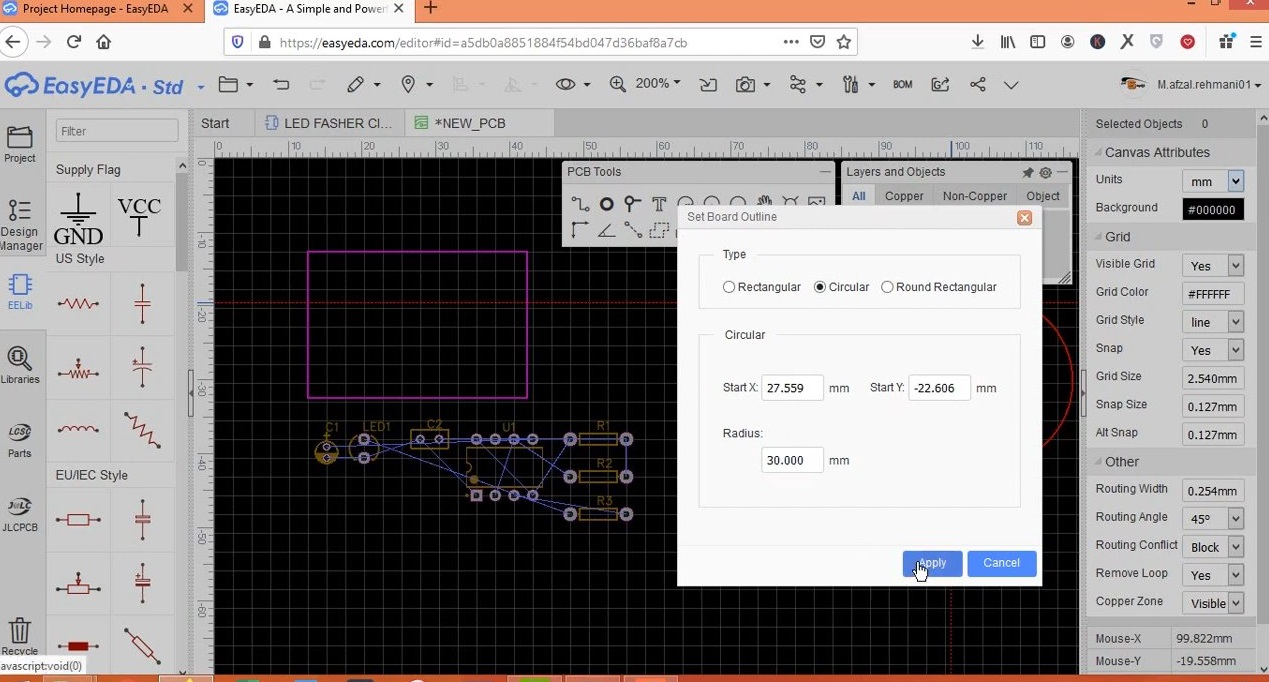
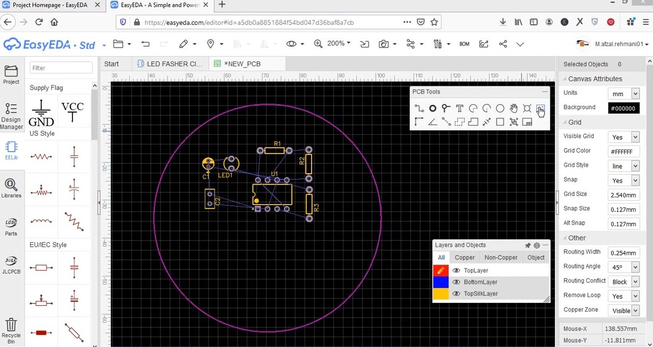
3) After that, Place all components within board outline
4) You can also place a logo on your PCB Card by selecting the image icon –> ‘Select image file’ & then choose your desired image from local drive. then drag the logo to the desired location on the PCB board (set the image attribute to ‘Top Silk Layer’ by right clicking & selecting attributes).
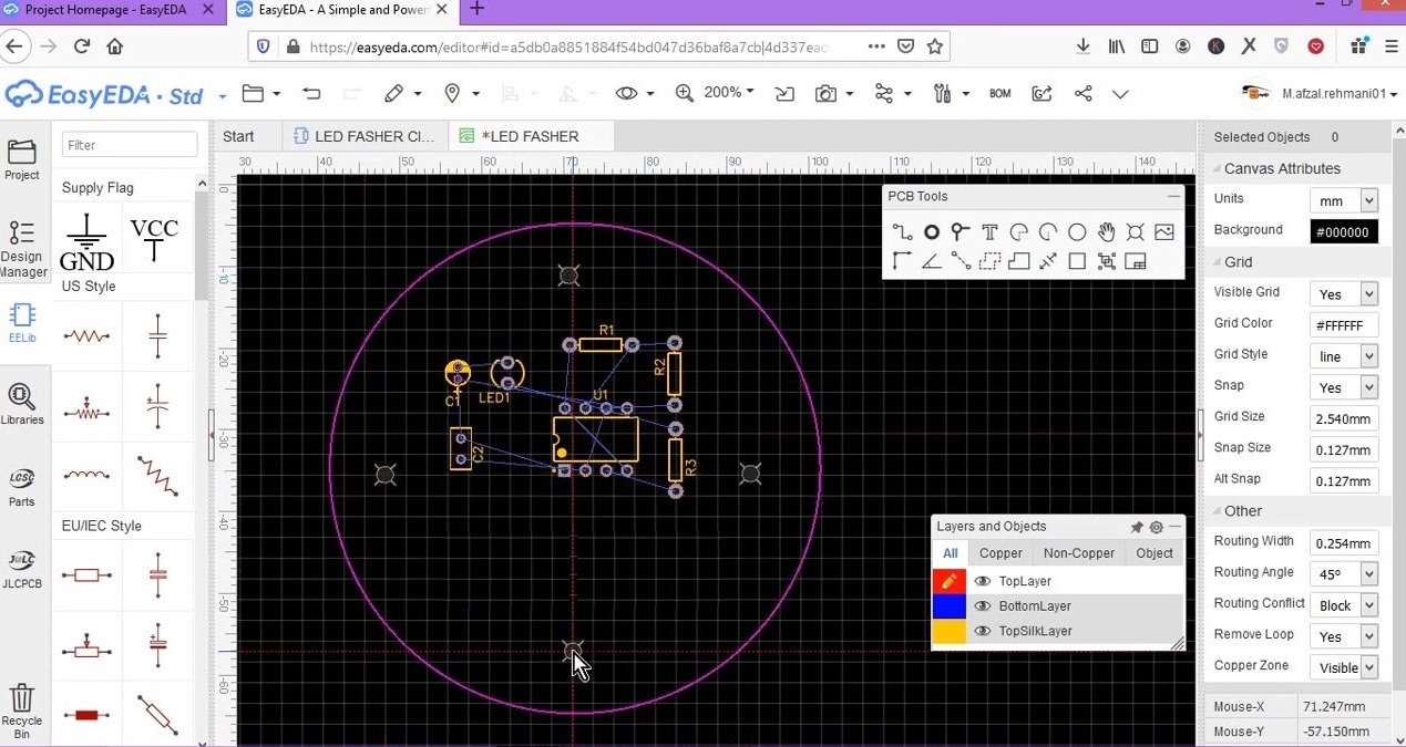
5) After that, If you need to mount the PCB on a device, then you can add mounting holes on the PCB board by clicking the ‘Hole’ icon in the PCB toolbox, then add the mounting holes.
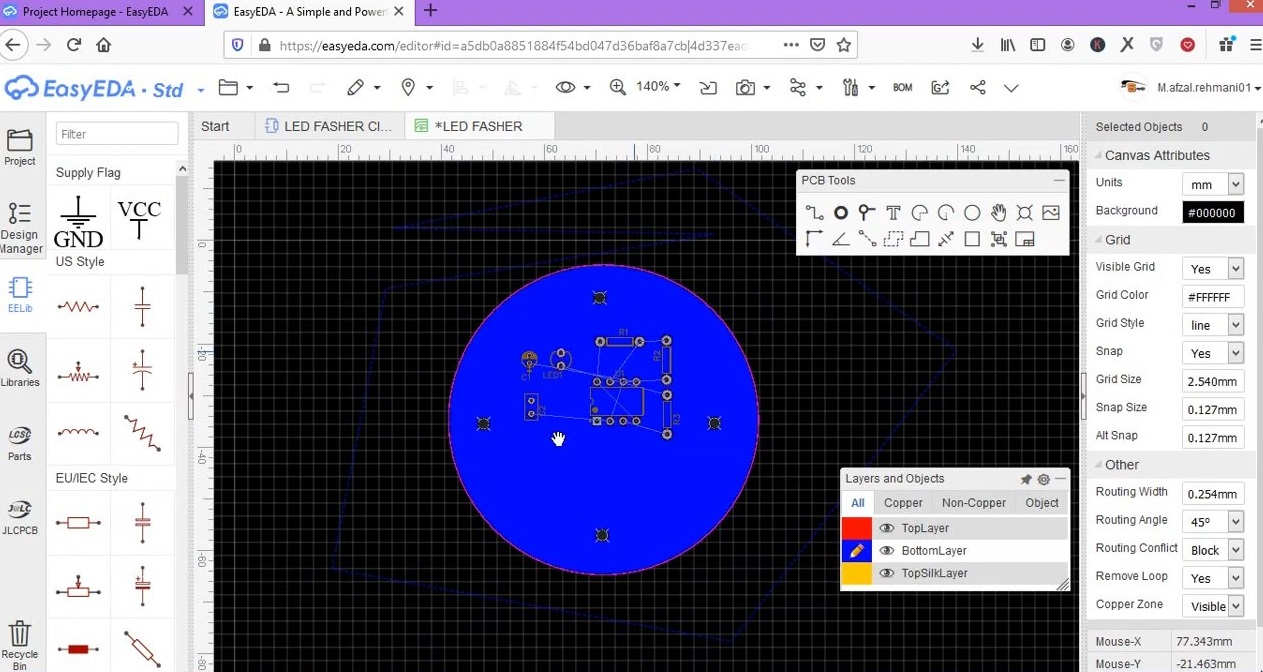
6) After that, map copper area beneath your PCB board outline by selecting the ‘Copper Area’ option from the PCB toolbox & tracing the area around the PCB Board outline and clicking the ‘move’ hand icon.
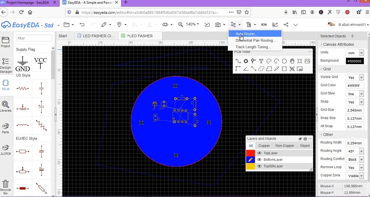
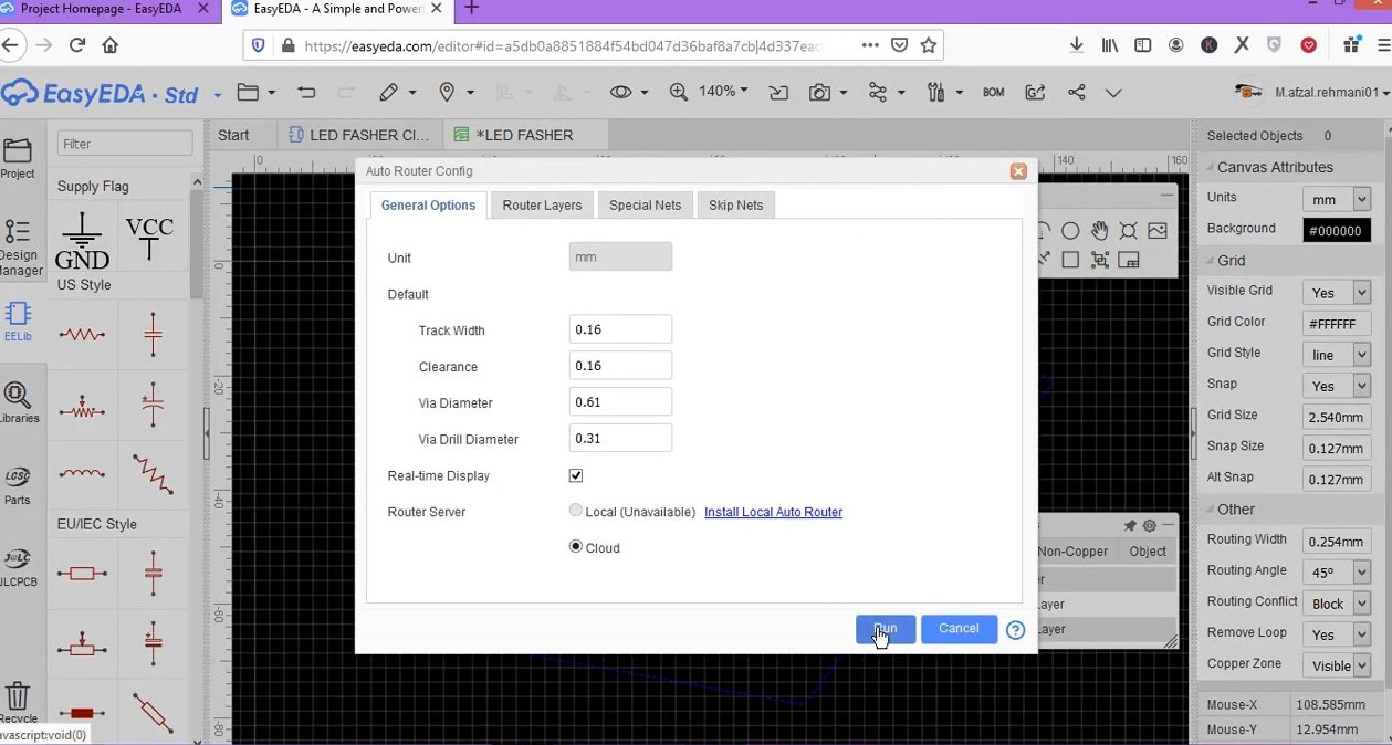
7) After that, run the Auto router by selecting the router option from the drop down menu.
8) After completing your design, select the 3D view from the dropdown menu to view the finished PCB.