
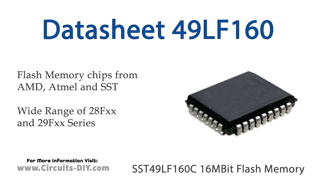
The SST49LF160C flash memory device is designed to interface with host controllers (chipsets) that support a low-pin-count (LPC) interface for system firmware applications. The SST49LF160C device complies with the LPC Interface Specification. The LPC interface operates with 5 signal pins versus 32 pins of 8-bit parallel flash memory. This frees up pins on the ASIC host controller resulting in lower ASIC costs and a reduction in overall system costs due to simplified signal routing.
The SST49LF160C uses a 5-signal LPC interface to support both in-system and rapid factory programming using programmer equipment. A high voltage pin (WP#/AAI) is used to enable Auto Address Increment (AAI) mode. The SST49LF160C offers hardware block protection in addition to individual block protection via software registers for critical system code and data. A 256-bit Security ID space with a 64-bit factory preprogrammed unique number and a 192-bit user programmable OTP area enhances the user’s ability to use new security techniques and implement a new data protection scheme.
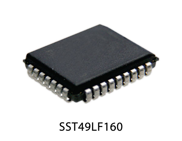
49LF160 Pinout
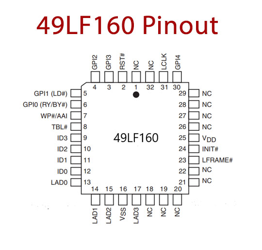
49LF160 Pin Configuration
| Pin No | Pin Name | Description |
|---|---|---|
| 1 | NC | Not Connect |
| 2 | RST | Reset Pin |
| 3 | GP13 | General Purpose Input 13 |
| 4 | GP12 | General Purpose Input 12 |
| 5 | GP11 | General Purpose Input 11 |
| 6 | GP10 | General Purpose Input 10 |
| 7 | WP | AAI Enable Pin |
| 8 | TBL | Top Block Lock Pin |
| 9 | ID3 | Identification Inputs 3 |
| 10 | ID2 | Identification Inputs 2 |
| 11 | ID1 | Identification Inputs 1 |
| 12 | ID0 | Identification Inputs 0 |
| 13 | LADO | Address and Data Pin 0 |
| 14 | LAD1 | Address and Data Pin 1 |
| 15 | LAD2 | Address and Data Pin 2 |
| 16 | VSS | Ground Pin |
| 17 | LAD3 | Address and Data Pin 3 |
| 18 | NC | Not Connect |
| 19 | NC | Not Connect |
| 20 | NC | Not Connect |
| 21 | NC | Not Connect |
| 22 | NC | Not Connect |
| 23 | L FRAME | Frame Pin |
| 24 | INIT | Initialize Pin |
| 25 | VDD | Power Supply Pin |
| 26 | NC | No Connection |
| 27 | NC | Not Connect |
| 28 | NC | Not Connect |
| 29 | NC | Not Connect |
| 30 | GP14 | General Purpose Input 14 |
| 31 | L CLK | Clock Pin |
| 32 | NC | Not Connect |
49LF160 Key Feature
- Conforms to LPC Interface Specification
- Support Single-Byte LPC Memory Read/Write Cycles
- Single 3.0-3.6V Read and Write Operations
- Superior Reliability
- Endurance: 100,000 Cycles (typical)
- Greater than 100 years Data Retention
- Low Power Consumption
- Active Read Current: 12 mA (typical)
- Standby Current: 10 µA (typical)
- Uniform 4 KByte sectors
- 35 Overlay Blocks: one 16-KByte Boot Block, two 8-
- KByte Parameter Blocks, one 32-Kbyte Parameter
- Block, thirty-one 64-KByte Main Blocks
You can download this datasheet for SST49LF160C 16MBit Flash Memory – Datasheet from the link given below: