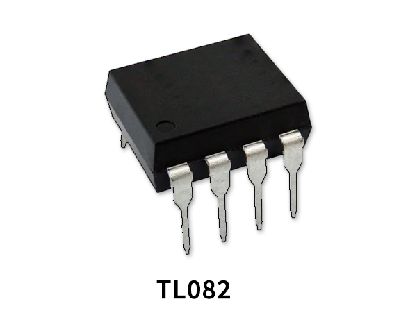
TL082 combines two state-of-the-art linear technologies on a single monolithic integrated circuit. Each internally compensated operational amplifier has well-matched high voltage JFET input devices for low input offset voltage. The IC has a range of working conditions a wide range of working voltages and possesses direct interfacing capability with almost every PMOS, CMOS, and NMOS device.
Operational Amplifier
Operational Amplifiers are basically voltage amplifying devices designed to be used with components like capacitors and resistors. They serve as the core part of any analog device. Feedback components like capacitors and resistors are used to determine the operation of the amplifier. The amplifier can perform many different operations (resistive, capacitive, or both), giving it the name Operational Amplifier. Op-amps are linear devices that are ideal for DC amplification and are used often in signal conditioning, filtering or other mathematical operations
TL082 Pinout
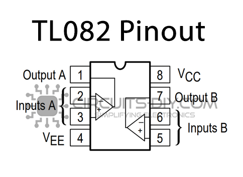
TL082 Pin Configuration
| Pin No | Pin Name | Description |
|---|---|---|
| 1 | OUTPUT A | Output Of Amplifier A |
| 2 | INV-INPUT A | Inverting Input Of Amplifier A |
| 3 | NON-INV-INPUT A | Non Inverting Input Of Amplifier A |
| 4 | VEE | Emitter Supply Voltage |
| 5 | NON-INV-INPUT B | Non Inverting Input Of Amplifier B |
| 6 | INV-INPUT B | Inverting Input Of Amplifier B |
| 7 | OUTPUT B | Output Of Amplifier B |
| 8 | VCC | Collector Supply Voltage |
TL082 Features
- Input Offset Voltage Options of 6.0 mV and 15 mV Max
- Low Input Bias Current: 30 pA
- Low Input Offset Current: 5.0 pA
- Wide Gain Bandwidth: 4.0 MHz
- High Slew Rate: 13 V/µs
- Low Supply Current: 1.4 mA per Amplifier
- High Input Impedance: 1012
Application
- Motor drives: AC and servo drive control and
- Power stage modules
- Single phase online UPS
- Three phase LIPS
- Pro audio mixers
- These devices are op amps with an internally trimmed input offset voltage and JFET input devices (BI-FET II). These JFETs have large reverse breakdown voltages from gate to source and drain eliminating the need for clamps across the inputs. Therefore, large differential input voltages can easily be accommodated without a large increase in input current. The maximum differential input voltage is independent of the supply voltages. However, neither of the input voltages should be allowed to exceed the negative supply as this will cause large currents to flow which can result in a destroyed unit.
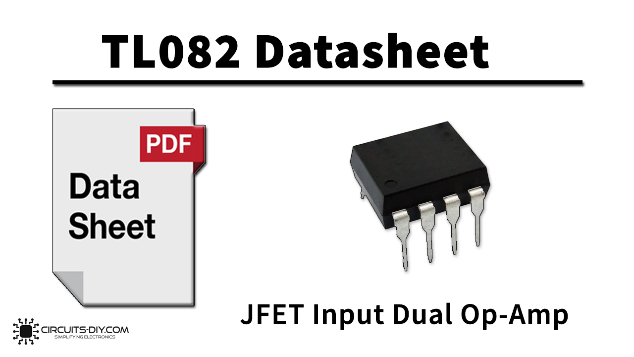
TL082 Datasheet
You can download this datasheet for TL082 JFET Input Dual Op-Amp from the link given below:
See Also: CD4584 Hex Schmitt Trigger – Datasheet | CD4536 Programmable Timer – Datasheet | CD4075 Triple 3-Input OR Gate – Datasheet