Contents
hide
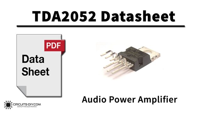
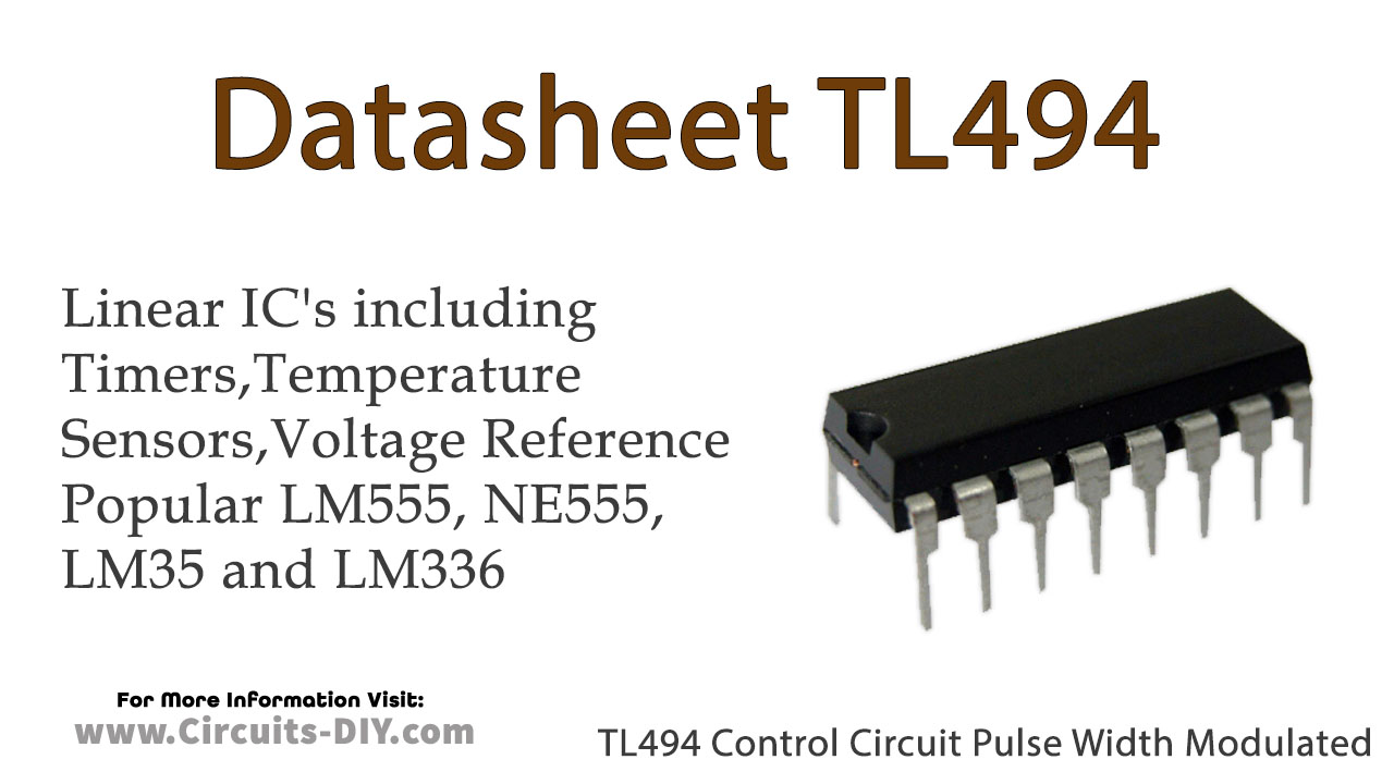
The TL494 is a fixed frequency, pulse width modulation control circuit designed primarily for switchmode power supply control.
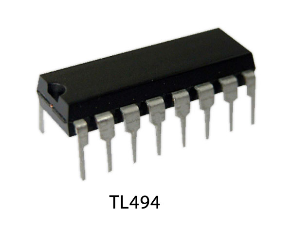
TL494 Pinout
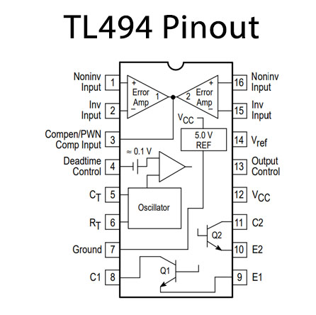
TL494 Pin Configuration
| Pin No | Pin Name | Description |
|---|---|---|
| 1 | N-INV | Non-Inverting Pin |
| 2 | INV | Inverting Pin |
| 3 | COMP: INPUT | Compensation Input Pin |
| 4 | DEADTIME CONTROL | Deadtime Control Pin |
| 5 | CT | Capacitor Timing Pin |
| 6 | RT | Resistor Timing Pin |
| 7 | GND | Ground Pin |
| 8 | C1 | Collector Pin 1 |
| 9 | E1 | Emitter Pin 1 |
| 10 | E2 | Emitter Pin 2 |
| 11 | C2 | Collector Pin 2 |
| 12 | VCC | Supply Voltage Pin |
| 13 | OUTPUT CONTROL | Output Control Pin |
| 14 | Vref | Reference Voltage Pin |
| 15 | INV | Inverting Pin |
| 16 | NON-INV | Non-Inverting Pin |
TL494 Features
- Complete Pulse Width Modulation Control Circuitry
- On–Chip Oscillator with Master or Slave Operation
- On–Chip Error Amplifiers
- On–Chip 5.0 V Reference
- Adjustable Deadtime Control
- Uncommitted Output Transistors Rated to 500 mA Source or Sink
- Output Control for Push–Pull or Single–Ended Operation
- Under voltage Lock out
You can download this datasheet for TL494 Control Circuit Pulse Width Modulated – Datasheet from the link given below: